Method of reducing leakage current using sleep transistors in programmable logic device

a technology of programmable logic and sleep transistor, which is applied in the direction of power consumption reduction, pulse technique, instruments, etc., can solve the problems of increasing static power consumption, large number of resources available on the pld, and unused pld resources, so as to reduce the leakage current in the pld, and minimize the effect of leakage curren

Inactive Publication Date: 2008-04-08
TAHOE RES LTD
View PDF2 Cites 26 Cited by
  • Summary
  • Abstract
  • Description
  • Claims
  • Application Information

AI Technical Summary

Benefits of technology

[0006]The PLD may be designed such that sleep transistors are associated with each logic element within the logic blocks in one to one correspondence. In this embodiment, a global sleep signal is distributed throughout the logic blocks and the logic elements within the logic blocks. In conjunction with a logic gate, and a CRAM bit, portions of the logic elements may be placed into sleep mode to further reduce the leakage current.
[0007]In another aspect of the invention, a method for reducing leakage current in a PLD is provided. The method includes applying a global sleep signal to the logical array blocks of the PLD. Then, a determination is made as to

Problems solved by technology

Consequently, a large number of resources available on the PLDs may remain unused and stay in stati

Method used


Image

  • Method of reducing leakage current using sleep transistors in programmable logic device
  • Method of reducing leakage current using sleep transistors in programmable logic device
  • Method of reducing leakage current using sleep transistors in programmable logic device

Examples


Embodiment Construction

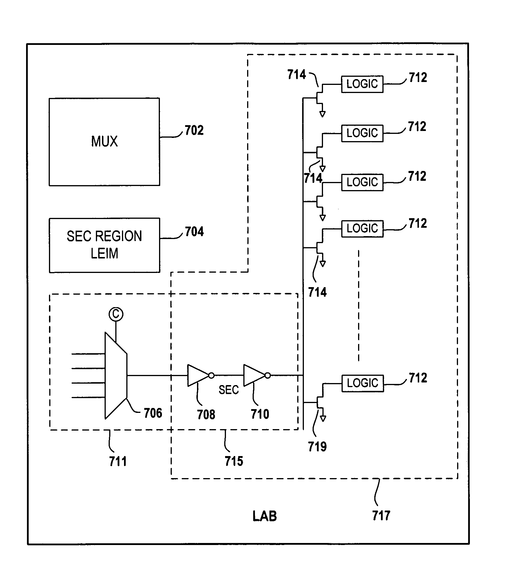
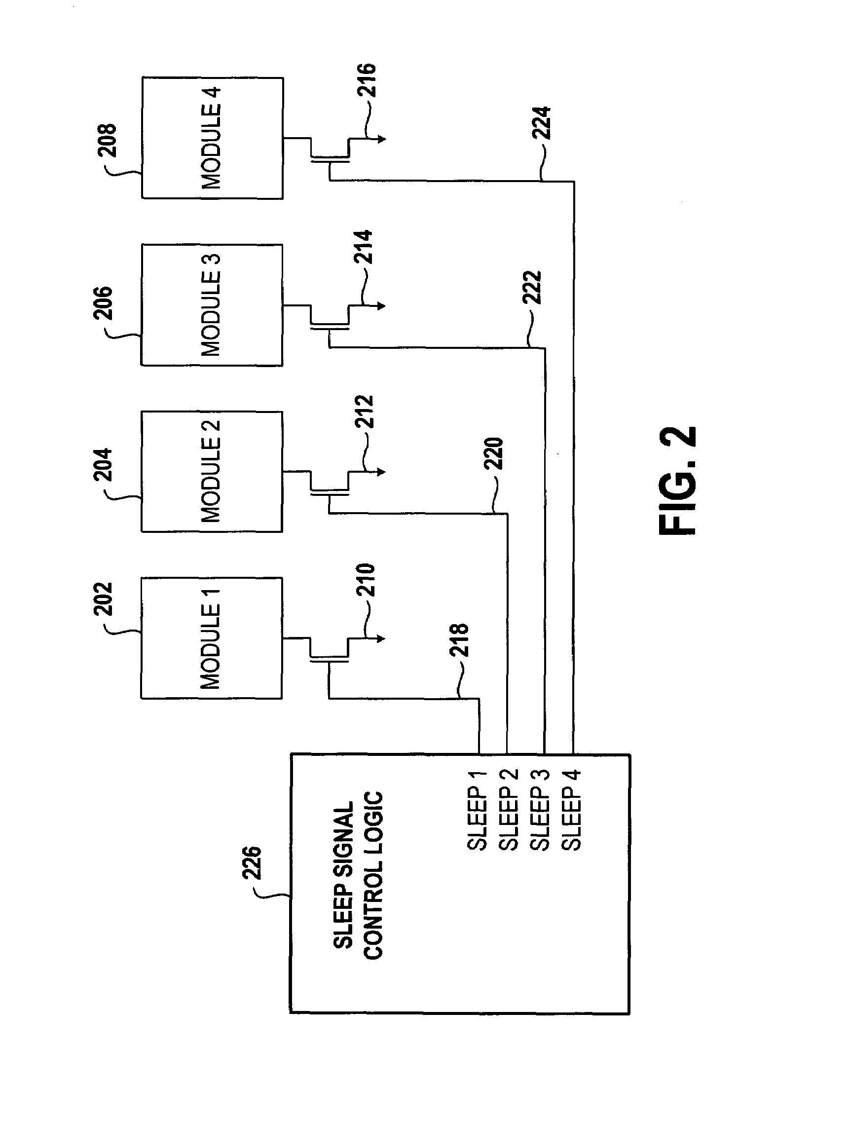
[0024]A method and system for reducing leakage current using sleep transistors is provided. The embodiments described herein provide sleep transistors for each element of the PLD so that every element in the PLD may be put into sleep mode. Alternatively, blocks of logic may be inactivated as described below. Moreover, the embodiments provide techniques to prevent nodes from floating, when the nodes are in electrical communication with external active regions within the PLDs.

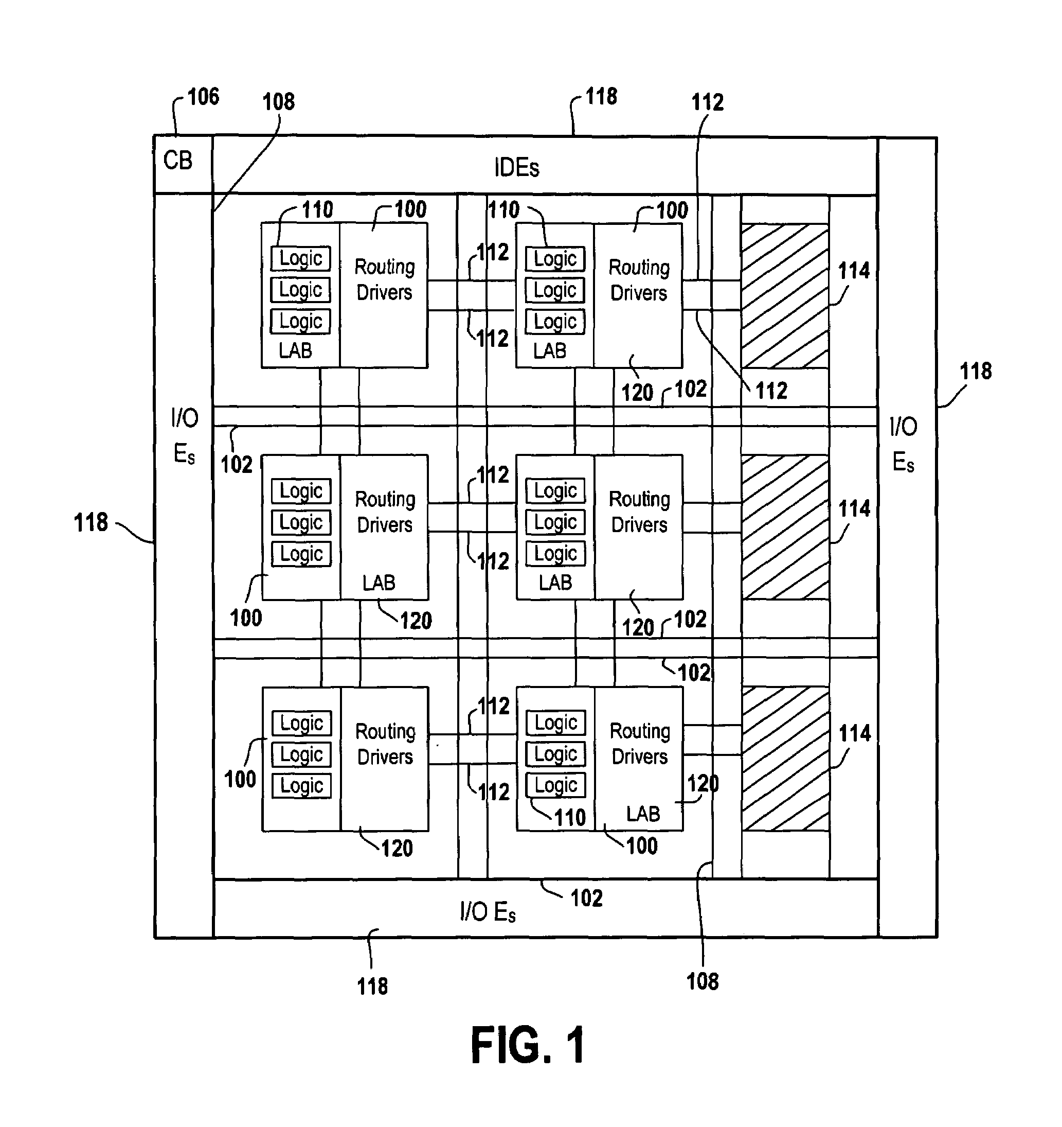
[0025]FIG. 1 is a simplified schematic diagram of the layout of a programmable logic device (PLD), in accordance with an embodiment of the invention. In one embodiment, the PLD is a Field Programmable Gate Array (FPGA). One skilled in the art will understand and appreciate that other types of PLDs may be used in place of FPGAs. The layout includes input / output circuitry blocks (IOEs) 118, logical array blocks 100, horizontal interconnects 102, vertical interconnects 108, control blocks 106, and memory blocks 114....


PUM


Abstract

A programmable logic device (PLD) having minimal leakage current for inactive logic blocks is provided. The PLD includes an array of logic blocks. Among the array of logic blocks, one of the array of logic blocks monitors the level of activity of each of the remaining logic blocks. The level of activity may be monitored by observing the input and output pin of the logic blocks. The PLD further includes a plurality of driven wires defining a routing pattern between the array of logic blocks. When one of the array of logic blocks detect inactivity in any one of the remaining logic blocks for a certain duration, the one of the array logic blocks transmits a signal invoking a sleep mode for the inactive logic blocks. A sleep transistor with a threshold voltage level that is capable minimizing the leakage current is associated with each of the remaining block. The gate of the sleep transistor receives the signal transmitted by one of the array logic blocks and the signal switches off the sleep transistor.

Description


Claims


Application Information

Patent Timeline
Owner TAHOE RES LTD
Why Eureka
Try Eureka