Thin array plastic package without die attach pad and process for fabricating the same

a technology of die-attaching pads and plastic packages, which is applied in the direction of semiconductor devices, electrical equipment, semiconductor/solid-state device details, etc., can solve the problem of low package profile and achieve the effect of small package assembly and low package profil

Active Publication Date: 2008-04-15
UTAC HEADQUARTERS PTE LTD
View PDF55 Cites 77 Cited by
  • Summary
  • Abstract
  • Description
  • Claims
  • Application Information

AI Technical Summary

Benefits of technology

[0010]In one aspect of the present invention, the integrated circuit package does not include a die attach pad. Advantageously, this results in a low package profile. In other advantages, extremely small package assembly is possible, and corner areas of the package are available for additional input / output (I / O).
[0011]In another aspect of the present invention, fiducial markings are created on the top surface of the substrate and these fiducial markings are visible through the use of a transparent mask. The substrate is mounted to a tape that backs a carrier, in a void in the carrier. Saw grooves singulate the integrated circuit packages. The saw grooves extend through the molding material and the substrate, ending at the tape such that the saw grooves extend at most only partly through the tape. Thus, the saw grooves extend from the top side of the packages of the strip, rather than the bottom side as in the prior art. The transparent mask permits visibility of the fiducial marks on the top side for sawing. Advantageously, the packages can be saw singulated while retaining the package on the tape, since the saw grooves do not extend through the tape. In another aspect, the tape is an ultraviolet (UV) light tape that is treated with UV light after mounting the substrate to the tape. Exposed portions of the tape become much less sticky after UV light treatment.

Problems solved by technology

Advantageously, this results in a low package profile.

Method used


Image

  • Thin array plastic package without die attach pad and process for fabricating the same
  • Thin array plastic package without die attach pad and process for fabricating the same
  • Thin array plastic package without die attach pad and process for fabricating the same

Examples


Embodiment Construction

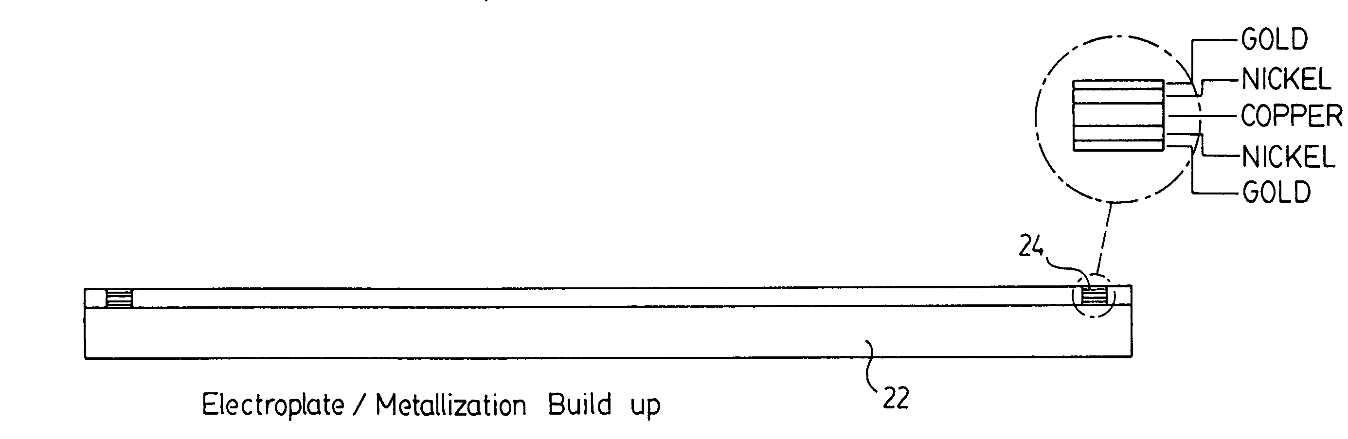
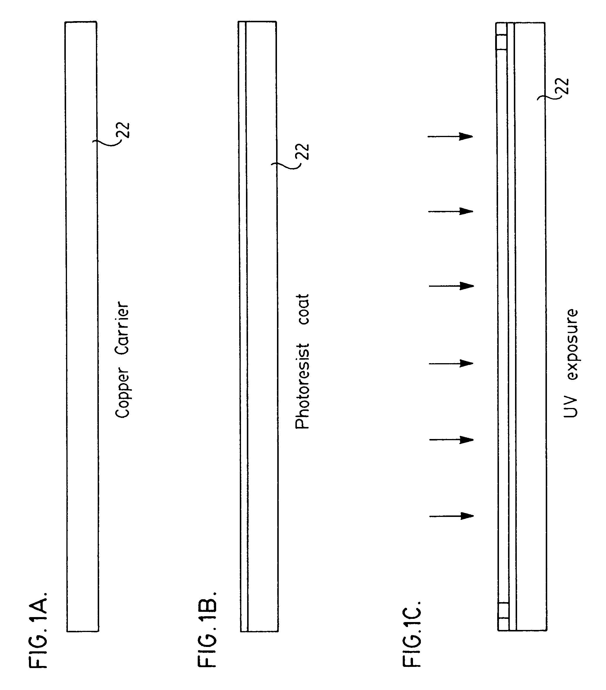
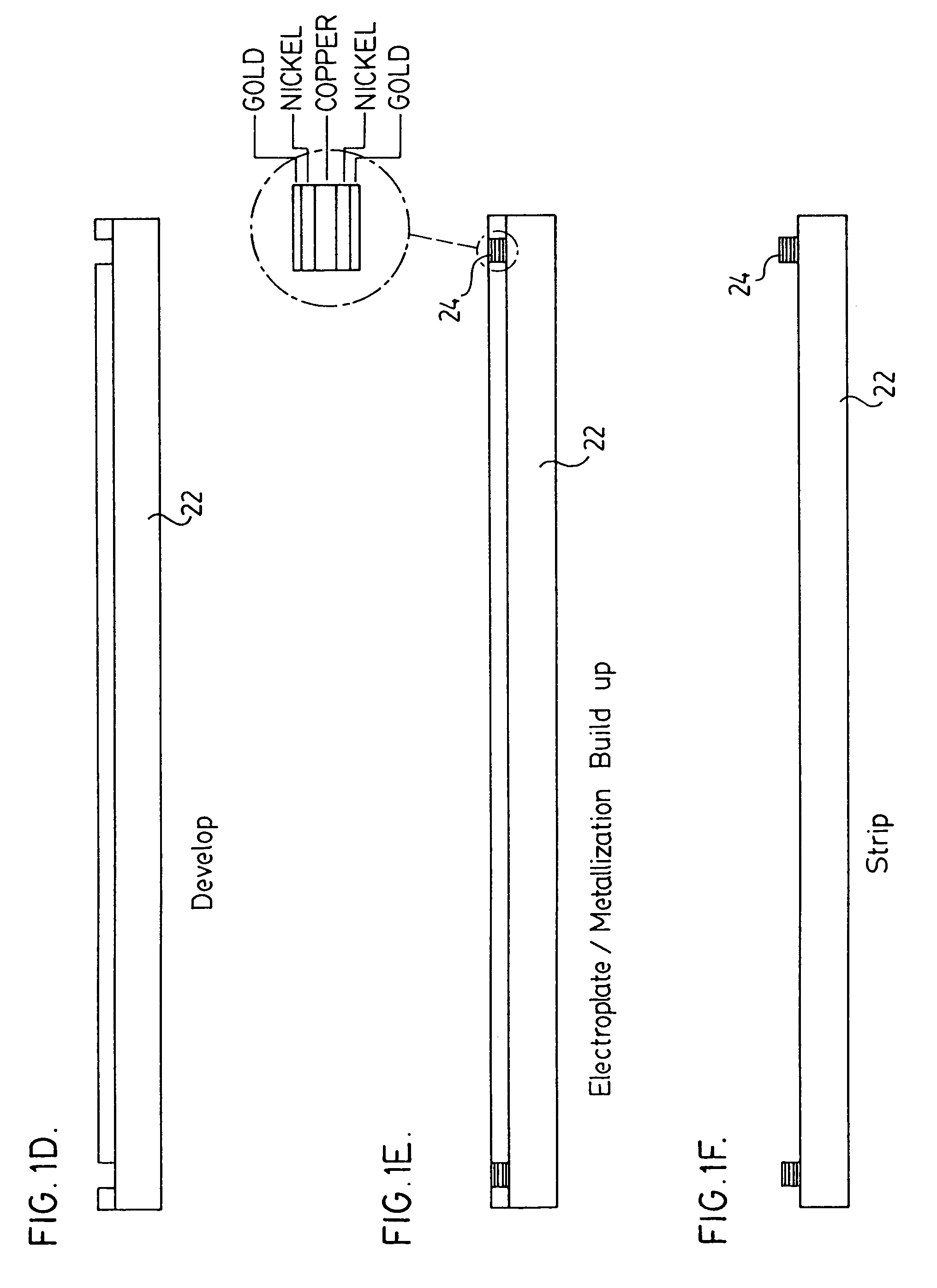
[0016]Reference is now made to the figures to describe a process for fabricating an integrated circuit package according to one embodiment of the present invention. The integrated circuit package is indicated generally by the numeral 20. Metal is plated up on a substrate 22 to provide a plurality of contacts pads 24 and a plurality of fiducial markings 26 on a periphery of the contact pads 24. A transparent mask 28 is selectively deposited on the substrate 22, over the fiducial markings 26. A semiconductor die 30 is mounted on the substrate 22 such that the contact pads 24 circumscribe the semiconductor die 30 and the semiconductor die 30 is wire bonded to ones of the contact pads 24. The wire bonds 32 are encapsulated and the semiconductor die 30 and contact pads 24 are covered in a molding material 34. The substrate 22 is selectively etched to thereby etch away the substrate 22 underneath the contact pads 24 and the semiconductor die 30. The integrated circuit package 20 is singul...


PUM


Abstract

A process for fabricating an integrated circuit package. Metal is plated up on a substrate to provide a plurality of contact pads and a plurality of fiducial markings on a periphery of the contacts. A transparent mask is selectively deposited on the substrate, over the fiducial markings. A semiconductor die is mounted on the substrate such that the contact pads circumscribe the semiconductor die and the semiconductor die is wire bonded to ones of the contact pads. The wire bonds are encapsulated and the semiconductor die and contact pads are covered in a molding material. The substrate is selectively etched to thereby etch away the substrate underneath the contact pads and the semiconductor die. The integrated circuit package is singulated from other integrated circuit packages by sawing using the fiducial markings.

Description

FIELD OF THE INVENTION[0001]The present invention relates in general to integrated circuit packaging and more particularly to a leadless plastic chip carrier that does not have a die attach pad and that includes a post-mold etch step to etch away a copper carrier.BACKGROUND OF THE INVENTION[0002]According to well known prior art IC (integrated circuit) packaging methodologies, semiconductor dice are singulated and mounted using epoxy or other conventional means onto respective die pads (attach paddles) of a leadframe strip. Traditional QFP (Quad Flat Pack) packages incorporate inner leads which function as lands for wire bonding the semiconductor die bond pads. These inner leads typically require mold locking features to ensure proper positioning of the leadframe strip during subsequent molding to encapsulate the package. The inner leads terminate in outer leads that are bent down to contact a mother board, thereby limiting the packaging density of such prior art devices.[0003]In or...

Claims


Application Information

Patent Timeline
Patent Type & Authority Patents(United States)
IPC IPC(8): H01L21/00
CPCH01L21/4832H01L23/3107H01L24/97H01L21/561H01L2924/01019H01L2223/54473H01L2224/1147H01L2224/48091H01L2224/49171H01L2224/92247H01L2224/97H01L2924/01029H01L2924/01046H01L2924/01078H01L2924/01079H01L2924/01082H01L2924/14H01L2924/18165H01L2224/73265H01L2224/48247H01L2224/45144H01L2924/01033H01L24/48H01L24/49H01L2924/01005H01L2924/00014H01L2224/85H01L2224/83H01L2924/00H01L24/45H01L2924/15747H01L2924/181H01L2924/00015H01L2224/05599H01L2924/00012
Inventor MCLELLAN, NEILPEDRON, SERAFINHIGGINS, III, LEO M.TSANG, KWOK CHEUNGKWAN, KIN PUI
Owner UTAC HEADQUARTERS PTE LTD
Why Eureka
Try Eureka