Unlock instant, AI-driven research and patent intelligence for your innovation.

Memory module and signal line arrangement method thereof

a memory module and signal line technology, applied in the field of memory modules, can solve the problems of signal distortion, method spatial limitation of signal line arrangement, long signal line from via to pad, etc., and achieve the effect of efficient transmission of high-frequency signals

Inactive Publication Date: 2008-06-24
SAMSUNG ELECTRONICS CO LTD
View PDF15 Cites 2 Cited by
  • Summary
  • Abstract
  • Description
  • Claims
  • Application Information

AI Technical Summary

Benefits of technology

[0010]It is an object of the present invention to provide a memory module which can efficiently transmit a high-frequency signal even though a via is arranged at a location that is in proximity to one of pads in contact with the same signal applying balls (pins) on both sides of the PCB.
[0011]It is another object of the present invention to provide a signal arrangement method of a memory module which can efficiently transmit a high-frequency signal even though a via is arranged at a location that is in proximity to one of pads in contact with the same signal applying balls (pins) on both sides of the PCB.

Problems solved by technology

However, this method has a spatial limitation to arranging signal lines arranged around the via since the via has to be located at a center of the pads to which the same signal applying balls (pins) arranged on both sides of the PCB in a mirror form contact.
Further, since a time for a signal to pass through the via is not considered, signal transmission times spent for a signal to be transmitted to the pads which the same signal applying balls (pins) arranged on both sides in a mirror form contact can differ, and thus if a signal which operates at a high frequency is transmitted, signal distortion can occur.
However, a length of the signal line from via to the pad can become lengthy because the via is arranged at a location close to one of the pads which the same signal applying balls (pins) contact.
Thus, this method has a limitation in that it is not conductive to transmit a high-frequency signal, like the first method for arranging the via at the central location of the same signal applying balls (pins) described above.

Method used


Image

  • Memory module and signal line arrangement method thereof
  • Memory module and signal line arrangement method thereof
  • Memory module and signal line arrangement method thereof

Examples


Embodiment Construction

[0029]The present invention will now be described more fully hereinafter with reference to the accompanying drawings, in which preferred embodiments of the invention are shown. This invention may, however, be embodied in different forms and should not be construed as limited to the embodiments set forth herein. Rather, these embodiments are provided so that this disclosure will be thorough and complete, and will fully convey the scope of the invention to those skilled in the art. In the drawings, the thickness of layers and regions are exaggerated for clarity. Like numbers refer to like elements throughout the specification.

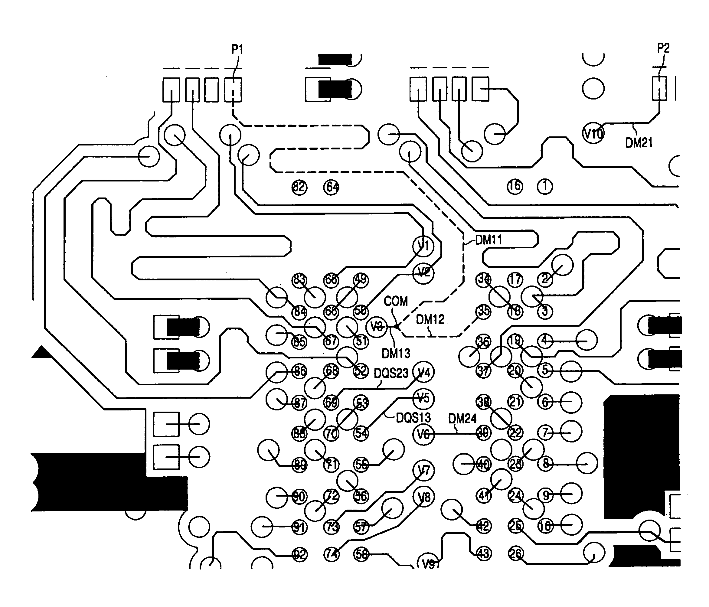
[0030]FIG. 1 is a schematic view illustrating a conventional memory module. A PCB of the memory module of FIG. 1 includes n layers 100-1 to 100-n. m memory chips 110-1 to 110-n are mounted on one side of the PCB, and m memory chips 120-1 to 120-m are mounted on the other side of the PCB in a mirror form, facing the m memory chips 110-1 to 110-m. Here, one side of...


PUM

PropertyMeasurementUnit
transmission timeaaaaaaaaaa
lengthaaaaaaaaaa
frequencyaaaaaaaaaa

Abstract

The pesent invention discloses a memory module and a signal line arrangement method thereof. The memory module includes memory chips mounted on both sidees in a mirror form; and a printed circuit board (PCB) having same signal applying contact pads arranged on both sodes which same signal applying balls of the memory chips contact in the mirror form, wherein a via is formed at a location close to the same signal applying contact pad of one side among the same signal applying contact pads arranged on both sides in the mirror form, the via connecting the other side to the signal line of one side, and a signal transmitted from the other side is connected to a contact junction, the contact junction is connected to the same signal applying contact pad of the other side, the contact junction is connected to the via of the other side, and the via of one side is connected to the same signal applying contact pad of one side.

Description

CROSS-REFERENCE TO RELATED APPLICATION[0001]This application claims the benefit of Korean Patent Application No. 2005-21552, filed Mar. 15, 2005, the disclosure of which is hereby incorporated herein by reference in its entirety.BACKGROUND OF THE INVENTION[0002]1. Field of the Invention[0003]The present invention relates to a memory module and, more particularly, to a memory module having memory chips on both sides thereof and a signal line arrangement method thereof.[0004]2. Description of the Related Art[0005]A memory module generally includes a printed circuit board (PCB) and memory chips. The memory chips mounted on the PCB can be arranged on both sides of the PCB in a mirrored configuration. That is, a same signal applying ball (pin) of each memory chip mounted on both sides of the PCB can be arranged on both sides of the PCB in a mirror form.[0006]A conventional signal line arrangement method includes forming a via passing through a central location of pads in contact with the...

Claims


Application Information

Patent Timeline
Patent Type & Authority Patents(United States)
IPC IPC(8): H05K1/16
CPCG11C5/025G11C5/04H05K1/181H05K1/112Y10T29/49155H05K2201/10159H05K2201/10545Y10T29/49128Y02P70/50
Inventor YOON, CHIL-NAMKIM, KWANG-SEOPKIM, DO-HYUNGLEE, JAE-JUNKO, KI-HYUN
Owner SAMSUNG ELECTRONICS CO LTD