Optical modulator module package using flip-chip mounting technology

a technology of optical modulator and module, applied in the field of optical modulator module package, can solve the problem of easy moisture inability of optical modulator device, and achieve the effect of convenient transmission and desirable optical characteristics

Inactive Publication Date: 2008-07-01
SAMSUNG ELECTRO MECHANICS CO LTD
View PDF5 Cites 19 Cited by
  • Summary
  • Abstract
  • Description
  • Claims
  • Application Information

AI Technical Summary

Benefits of technology

[0013]Accordingly, the present invention has been made keeping in mind the above problems occurring in the prior art, and an object of the present invention is to provide an optical modulator module package using a flip-chip mounting technology, in which an optical modulator device is optimally hermetically mounted, an electrical signal is easily transmitted, and desirable optical characteristics are maintained. In the present invention, electric interconnection and hermetic mounting are simultaneously achieved through a single process.
[0017]In another preferred embodiment, in the optical modulator module package using the flip-chip mounting technology according to the present invention, it is preferable that the upper metal pads of the optical modulator device and the lower metal pads of the light transmissive cover be connected to each other using an anisotropic conductive film (ACF) or a non-conductive film (NCF) so as to avoid bending of the device or nonuniform heights of bumps, thus assuring stable performance.

Problems solved by technology

Particularly, an optical modulator device is susceptible to moisture due to movement of active devices, thus hermetic mounting is necessary.

Method used


Image

  • Optical modulator module package using flip-chip mounting technology
  • Optical modulator module package using flip-chip mounting technology
  • Optical modulator module package using flip-chip mounting technology

Examples


second embodiment

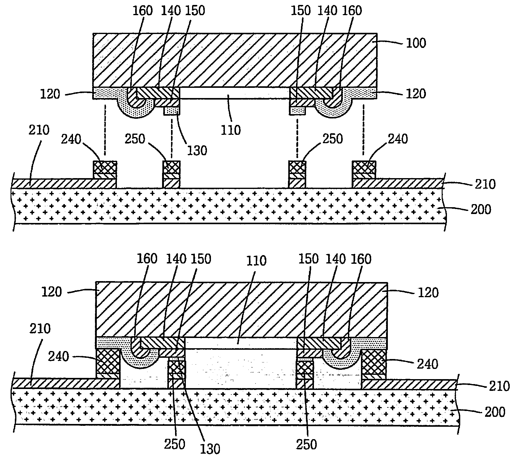
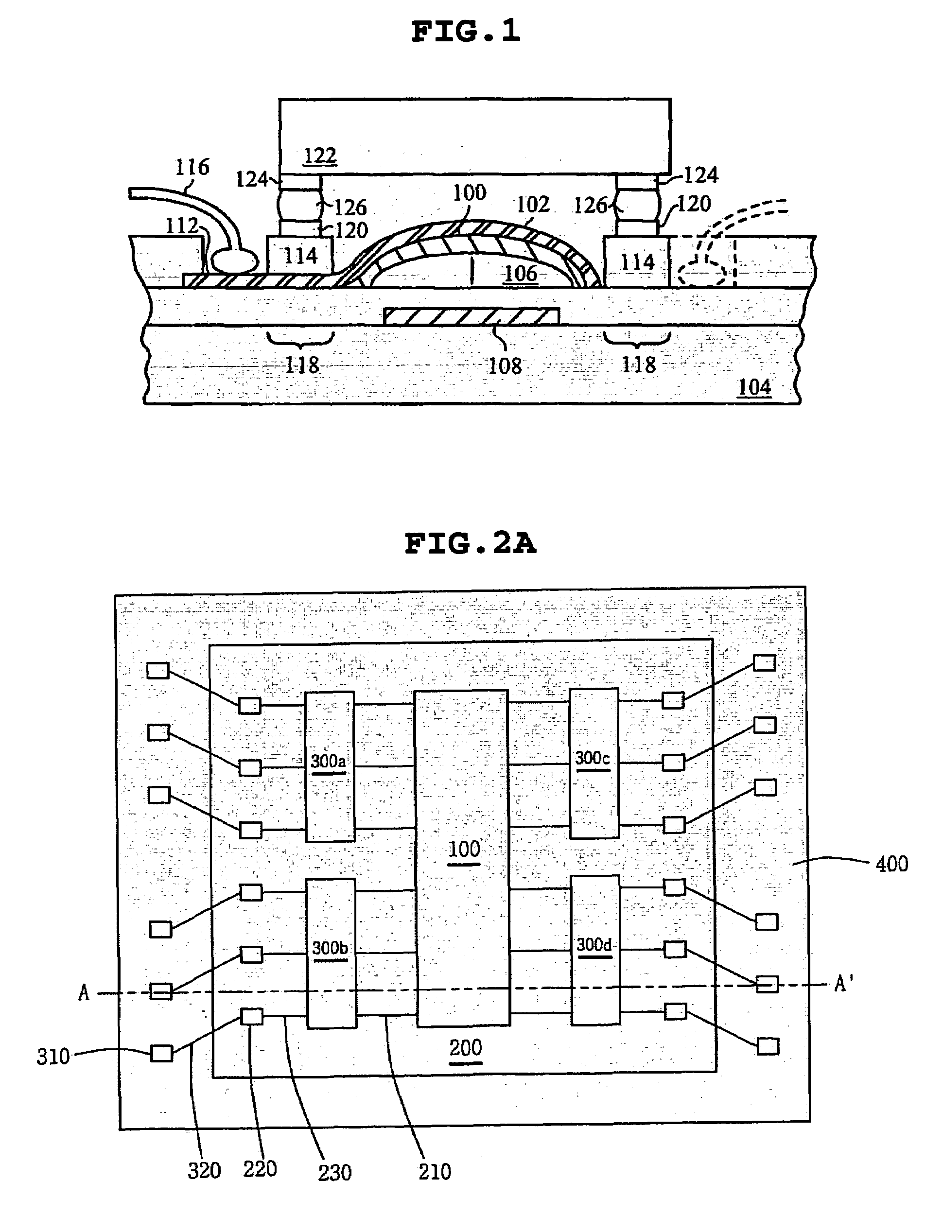
[0072]FIG. 10 is a sectional view illustrating attachment of an optical modulator device to a light transmissive cover using solder balls according to the present invention.

[0073]As shown in FIG. 10, an optical modulator device 1100 according to the second embodiment of the present invention comprises micromirrors 1110, upper metal pads 1120, an upper sealing pad 1130, lead wires 1140, and insulating layers 1150, 1160. A light transmissive cover 1200 comprises circuit patterns 1210, lower metal pads 1240, and a lower sealing pad 1250.

[0074]In the optical modulator module package according to the second embodiment of the present invention, the upper and lower sealing pads 1130, 1250 are connected using solder balls 1260, thus more reliable sealing is achieved. Furthermore, the upper and lower metal pads 1120, 1240 are connected using the solder balls 1260, thus more reliable electric connection is achieved.

third embodiment

[0075]FIG. 11 is a sectional view illustrating attachment of an optical modulator device to a light transmissive cover using anisotropic conductive films according to the present invention.

[0076]As shown in FIG. 11, an optical modulator device 2100 according to the third embodiment of the present invention comprises micromirrors 2110, upper metal pads 2120, an upper sealing pad 2130, lead wires 2140, and insulating layers 2150, 2160. A light transmissive cover 2200 comprises circuit patterns 2210, lower metal pads 2240, and a lower sealing pad 2250.

[0077]In the optical modulator module package according to the third embodiment of the present invention, the upper and lower metal pads 2120, 2240 or the upper and lower sealing pads 2130, 2250 are connected to each other using anisotropic conductive films 2260, thus a load applied to the optical modulator device 2100 or the light transmissive cover 2200 is reduced; thereby it is possible to prevent the optical modulator device 2100 or t...


PUM


Abstract

Disclosed herein is an optical modulator module package using a flip-chip mounting technology, in which an optical modulator device is hermetically mounted using the flip-chip mounting technology. The optical modulator device is protected from an external environment, it is easy to transmit an electrical signal to the exterior, and optical characteristics of the optical modulator device are desirably maintained.

Description

BACKGROUND OF THE INVENTION[0001]1. Field of the Invention[0002]The present invention relates, in general, to an optical modulator module package and, more particularly, to an optical modulator module package using a flip-chip mounting technology, in which easy electrical signal transmission between an optical modulator device and driver integrated circuits and hermetic mounting to desirably maintain characteristics of the optical modulator device are simultaneously achieved using the flip-chip mounting technology.[0003]2. Description of the Related Art[0004]Recently, many applications and products have been developed using a micro electromechanical system (MEMS) technology, and are used in daily life.[0005]Most MEMS products comprise movable components, and are affected by surface energy rather than energy caused by mass, due to a micrometer(μm)-sized fine structure.[0006]Accordingly, in order to assure stable and reliable performance of the products, movement of movable structures...

Claims


Application Information

Patent Timeline
Patent Type & Authority Patents(United States)
IPC IPC(8): H01L27/14H01L31/00
CPCG02B26/0833G03H2225/24H01L2224/16H01L2224/48091H01L2224/48463H01L2924/00014H01L2924/1461H01L2224/05568H01L2224/05023H01L2224/05001H01L2224/051H01L2224/056H01L2224/05553H01L24/05E04C3/293E04C5/06
Inventor PARK, HEUNG WOOLEE, YEONG GYUHONG, SUK KEEPARK, CHANG SULIM, OHK KUN
Owner SAMSUNG ELECTRO MECHANICS CO LTD
Why Eureka
Try Eureka