Image sensor module with optical path delimiter and accurate alignment

a technology of image sensor and path delimiter, which is applied in the direction of spurs, instruments, printing, etc., can solve the problems of damage signal processor and the like, and the accuracy of lens alignment with respect to solid-state image sensor is decreased, so as to achieve the effect of reducing the accuracy of lens alignmen

Inactive Publication Date: 2008-07-08
SHARP KK
View PDF22 Cites 14 Cited by
  • Summary
  • Abstract
  • Description
  • Claims
  • Application Information

AI Technical Summary

Benefits of technology

[0008]However, according to the imaging module described in Japanese Patent Application Laid-Open No. 2000-125212, since the lens frame material holding the lens is bonded onto the ceramic board and the ceramic board is large in manufacturing nonuniformity, when distortion occurs due to warpage, flexure or the like on the plane of the ceramic board serving as the reference plane, the accuracy of the alignment of the lens with respect to the solid-state image sensor is decreased. Likewise, according to the image sensor module described in Japanese Patent Application Laid-Open No. 2004-40287, since the housing holding the lens is bonded onto the board, when distortion occurs on the board, the alignment accuracy of the lens is decreased.
[0009]According to the optical device module described in Japanese Patent Application Laid-Open No. 2004-301938, since the lens holder is bonded to the transparent lid bonded onto the solid-state image sensor and the solid-state image sensor and the transparent lid are bonded together by a sheet-form bonding agent, the transparent lid can be bonded to the solid-state image sensor with high accuracy, and the accuracy of the alignment of the lens with respect to the solid-state image sensor is high. However, since the signal processor, the solid-state image sensor and the transparent lid are placed one on another on the board and the lens holder is further bonded to the transparent lid, there is a possibility that the solid-state image sensor, the signal processor and the like are damaged due to a shock given to the lens holder.

Problems solved by technology

However, according to the imaging module described in Japanese Patent Application Laid-Open No. 2000-125212, since the lens frame material holding the lens is bonded onto the ceramic board and the ceramic board is large in manufacturing nonuniformity, when distortion occurs due to warpage, flexure or the like on the plane of the ceramic board serving as the reference plane, the accuracy of the alignment of the lens with respect to the solid-state image sensor is decreased.
However, since the signal processor, the solid-state image sensor and the transparent lid are placed one on another on the board and the lens holder is further bonded to the transparent lid, there is a possibility that the solid-state image sensor, the signal processor and the like are damaged due to a shock given to the lens holder.
When the bonding agent is applied, it is difficult to make the thickness of the bonding agent uniform, there is a possibility that an error occurs in the lens position because of an error of the thickness of the bonding agent, and there is a possibility that excess bonding agent extends to the optical path and is captured in the image.

Method used


Image

  • Image sensor module with optical path delimiter and accurate alignment
  • Image sensor module with optical path delimiter and accurate alignment
  • Image sensor module with optical path delimiter and accurate alignment

Examples


Embodiment Construction

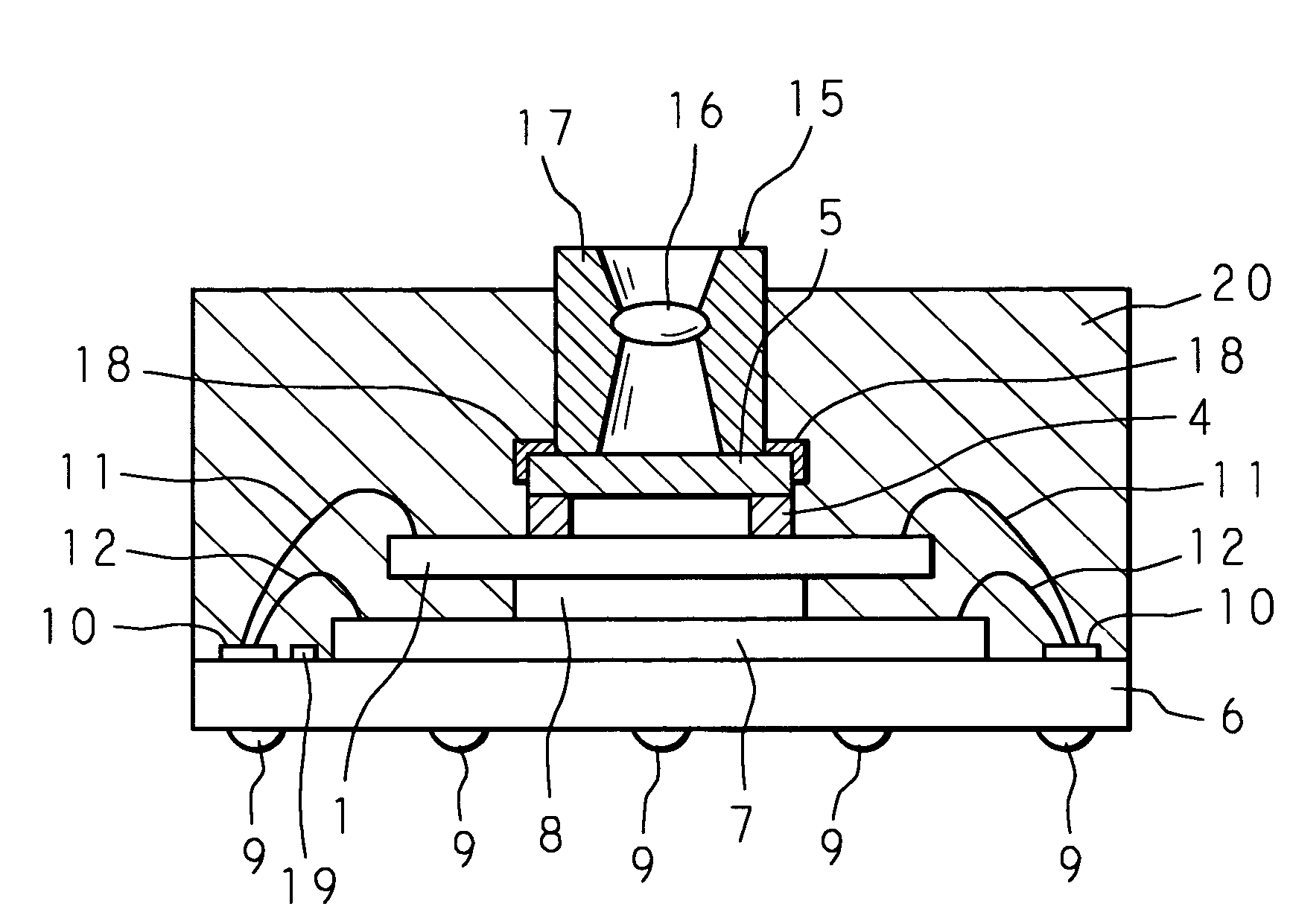
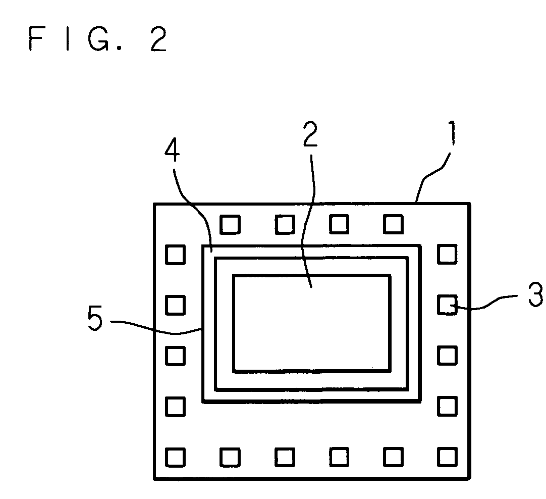
[0042]Hereinafter, the present invention will be concretely described with reference to the drawings showing an embodiment thereof. FIG. 1 is a schematic cross-sectional view showing the structure of an optical device module according to the present invention. FIG. 2 is a plan view of a solid-state image sensor according to the present invention. FIG. 3 is a side view showing the appearance of the optical device module according to the present invention. FIG. 4 is a plan view showing the appearance of the optical device module according to the present invention. FIG. 5 is a perspective view showing the structure of an optical path delimiter of the optical device module according to the present invention.

[0043]The optical device module according to the present invention includes a solid-state image sensor 1 that receives external light, a transparent lid 5 that protects the solid-state image sensor 1, a DSP 7 serving as the signal processor, and an optical path delimiter 15 that dire...


PUM


Abstract

An optical path delimiter having a lens is disposed so as to be in contact with a transparent lid bonded to a surface of a solid-state image sensor, and is fixed without bonded. Further, the solid-state image sensor to which the transparent lid is bonded, the optical path delimiter disposed so as to be in contact with the transparent lid without bonded, a DSP serving as a signal processor, a circuit part and a wiring board are fixed by being sealed in a synthetic resin. Even when distortion occurs due to warpage, flexure or the like on a board where the solid-state image sensor is disposed, the accuracy of the alignment of the lens with respect to the solid-state image sensor never decreases. In addition, the solid-state image sensor or the signal processor is never damaged by an external shock.

Description

CROSS-REFERENCE TO RELATED APPLICATIONS[0001]This Nonprovisional application claims priority under 35 U.S.C §119(a) on Patent Application No. 2005-95571 filed in Japan on Mar. 29, 2005, the entire contents of which are hereby incorporated by reference.BACKGROUND OF THE INVENTION[0002]The present invention relates to an optical device module incorporated in digital cameras, camera phones and the like and having a solid-state image sensor for photographing a subject, and a method of fabricating the optical device module.[0003]A solid-state image sensor provided in digital cameras, digital video cameras, camera phones and the like is for capturing the subject to be photographed. The solid-state image sensor is integrated into a module together with a lens, an infrared intercepting material and a signal processor processing the electric signal converted from captured image by the image sensor, and is provided as an optical device module. In recent years, digital cameras, camera phones a...

Claims


Application Information

Patent Timeline
Patent Type & Authority Patents(United States)
IPC IPC(8): H01L27/00H01L23/12H01L27/14
CPCH01L27/14618H01L27/14625H01L31/0203H01L2224/48227H01L2924/15311H01L2224/48091H01L2924/00014A43B13/24A43B5/185A43C17/04A43B13/30
Inventor TSUKAMOTO, HIROAKIHIROSUMI, NOBUHITOYASUDOME, TAKASHIKINOSHITA, KAZUO
Owner SHARP KK
Why Eureka
Try Eureka