Black level correcting device and electronic camera

a technology of black level correction and electronic camera, which is applied in the direction of color signal processing circuits, instruments, television systems, etc., can solve the problems of complex circuit structure and occurrence of sags, and achieve the effect of reducing sags in the devi

Inactive Publication Date: 2008-10-07
NIKON CORP
View PDF13 Cites 16 Cited by
  • Summary
  • Abstract
  • Description
  • Claims
  • Application Information

AI Technical Summary

Benefits of technology

[0016]An object of the present invention is to reduce a sag in a device for determining a black level of an image signal output from an image sensor, and an electronic camera in which this device is installed.
[0017]Another object of the present invention is to simplify the structure of a circuit in a device for determining a black level of an image signal output from an image sensor.
[0019]Therefore, according to the present invention, it is possible to expect the effect of shortening clamp time of the holding section, and stabilizing the maintaining level at a convergence level before starting the readout of the pixel signals from the valid pixels. As a result, it is possible to expect reduction in a sag.

Problems solved by technology

As a result, there is a problem of the occurrence of a sag (a direct-current standard level in the image signal varies because a time constant of a path is short).
As a result, there is a problem that the structure of the circuit is complicated.

Method used


Image

  • Black level correcting device and electronic camera
  • Black level correcting device and electronic camera
  • Black level correcting device and electronic camera

Examples


Embodiment Construction

[0031]An embodiment of the present invention will be hereinafter described with reference to the drawings. The same reference numbers as in the conventional art refer to identical components.

[0032]

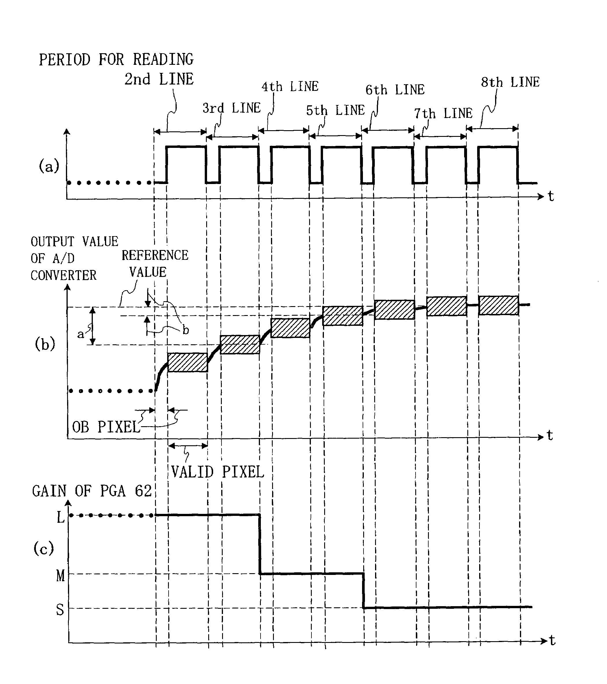
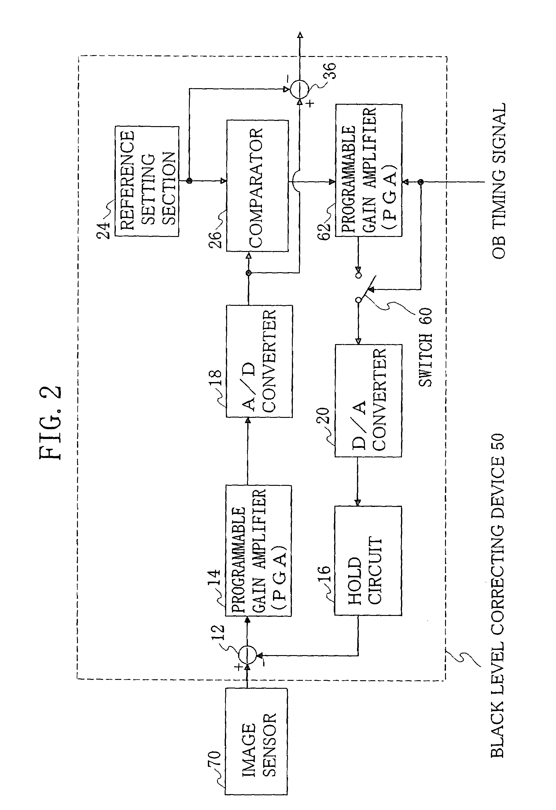
[0033]FIG. 2 is a block diagram of a black level correcting device according to this embodiment. A black level correcting device 50 has a subtracter 12, a PGA 14, a hold circuit 16, an A / D converter 18, a D / A converter 20, a switch 60, a PGA 62, a comparator 26, a reference setting section 24, and a subtracter 36. The function of each part of the black level correcting device 50 will be hereinafter described.

[0034]The subtracter 12 receives an analog pixel signal from an image sensor 70, and subtracts a hold level of the hold circuit 16 from the pixel signal to input the result into the PGA 14.

[0035]The PGA 14 amplifies the input analog pixel signal, and inputs the amplified pixel signal into the A / D converter 18.

[0036]The A / D converter 18 converts the input pixel signal to a digital pixel...


PUM


Abstract

A black level correcting device includes: an A / D converting section converting a result of subtracting a feedback signal from an input pixel signal into a pixel value to be output; and a feedback controlling section generating the feedback signal and having a holding section, a feedback gain adjusting section, etc. The holding section clamps a maintaining level to the level of the feedback signal while pixel signals of OB pixels are output, and maintains and outputs the maintaining level while pixel signals of valid pixels are output. The feedback gain adjusting section multiplies the feedback signal by clamp accelerating gain in synchronization with starting readout of the pixel signals from the OB pixels. Accordingly, clamp time of the holding section is shortened, enabling stabilization of the maintaining level at a convergence level before starting readout of the pixel signals from the valid pixels. Consequently, a sag can be reduced.

Description

CROSS-REFERENCE TO RELATED APPLICATIONS[0001]This application is based upon and claims the benefit of priority from Japanese Patent Application No. 2003-312238, filed on Sep. 4, 2003, the entire contents of which are incorporated herein by reference.BACKGROUND OF THE INVENTION[0002]1. Field of the Invention[0003]The present invention relates to technologies for determining a black level in an image signal.[0004]2. Description of the Related Art[0005]An image sensor generally has pixels shielded from light (optical black, hereinafter called OB pixels). A pixel signal output from this OB pixel is used for determining a signal level corresponding to black (hereinafter called a black level) (refer to, for example, Japanese Unexamined Patent Application Publication No. Hei 5-153429).[0006]FIG. 1 is a block diagram showing an example of a conventional black level correcting device. As shown in the drawing, a black level correcting device 10 has a subtracter 12, a programmable amplifier 14...

Claims


Application Information

Patent Timeline
Patent Type & Authority Patents(United States)
IPC IPC(8): H04N9/64G06K9/38H04N1/38H04N1/40H04N5/16H04N5/243H04N5/335H04N5/361H04N5/372H04N5/378H04N101/00
CPCH04N5/361H04N5/378H04N25/63H04N25/75
Inventor MORI, YOSHIZO
Owner NIKON CORP
Why Eureka
Try Eureka