Method of determining voltage compensation for flash memory devices

a voltage compensation and flash memory technology, applied in the field of memory devices, can solve the problems of reducing speed and cost, reducing data storage density, and unable to erase easily, so as to achieve faster erase operations, uniform threshold voltage distribution, and better programming

Active Publication Date: 2008-10-21
INFINEON TECH LLC +1
View PDF29 Cites 219 Cited by
  • Summary
  • Abstract
  • Description
  • Claims
  • Application Information

AI Technical Summary

Benefits of technology

[0018]The present invention determines or identifies programming variations for different groups of memory cells within an array or memory device that adequately program memory cells within the respective groups. Then, during programming operations for a given memory cell, programming voltages are applied according to the determined or identified programming variations for the group to which the given memory cell belongs. These adjusted programming variations result in relatively better programming, in terms of successful programs, data integrity, and the like, than conventional programming methods that employ a single set of programming voltages for an array or device. Additionally, the adjusted programming variations yield a relatively more uniform threshold voltage distribution. As a result, faster erase operations can be performed, which provides improved endurance characteristics and reliability.
[0019]For a given dual bit flash memory device, a portion of memory cells of the device are characterized to identify programming variations or adjustments. Subsequently, the memory cells are segmented into groups according to identified programming variations and, optionally, other properties such as location on the device. During programming of a particular memory cell, an associated group of which the particular cell is a member of is identified and programming voltages are obtained from the associated group. The memory cell is programmed with the obtained programming voltages with improved programming results, such as data integrity, programming success rate, and the like, as compared with conventional programming methods that treat all memory cells of a device or array identically during programming.

Problems solved by technology

For example, DRAM and SRAM allow individual bits of data to be erased one at a time, but such memory loses its data when power is removed.
EEPROM can alternatively be easily erased without extra exterior equipment, but has reduced data storage density, lower speed, and higher cost.
EPROM, in contrast, is less expensive and has greater density but lacks ease of erasability.
Such programming failures can result in problems including loss of time as a result of re-programming operations, loss of data, and the like.

Method used


Image

  • Method of determining voltage compensation for flash memory devices
  • Method of determining voltage compensation for flash memory devices
  • Method of determining voltage compensation for flash memory devices

Examples


Embodiment Construction

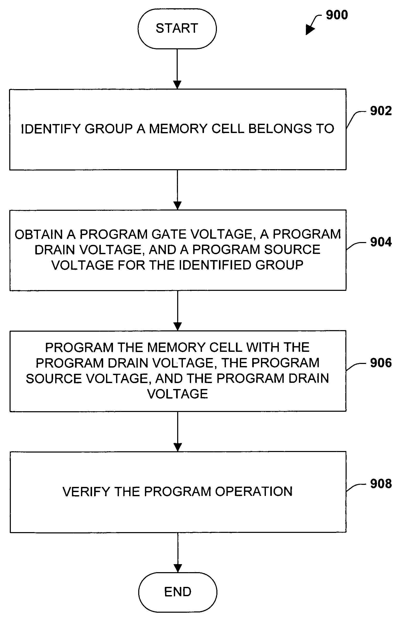
[0031]One or more aspects of the present invention are described with reference to the drawings, wherein like reference numerals are generally utilized to refer to like elements throughout, and wherein the various structures are not necessarily drawn to scale. In the following description, for purposes of explanation, numerous specific details are set forth in order to provide a thorough understanding of one or more aspects of the present invention. It may be evident, however, to one skilled in the art that one or more aspects of the present invention may be practiced with a lesser degree of these specific details. In other instances, well-known structures and devices are shown in block diagram form in order to facilitate describing one or more aspects of the present invention.

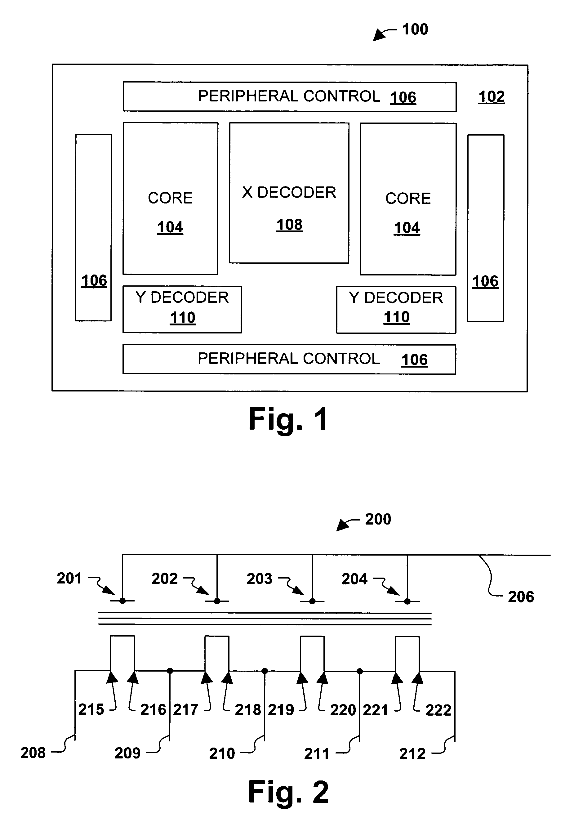
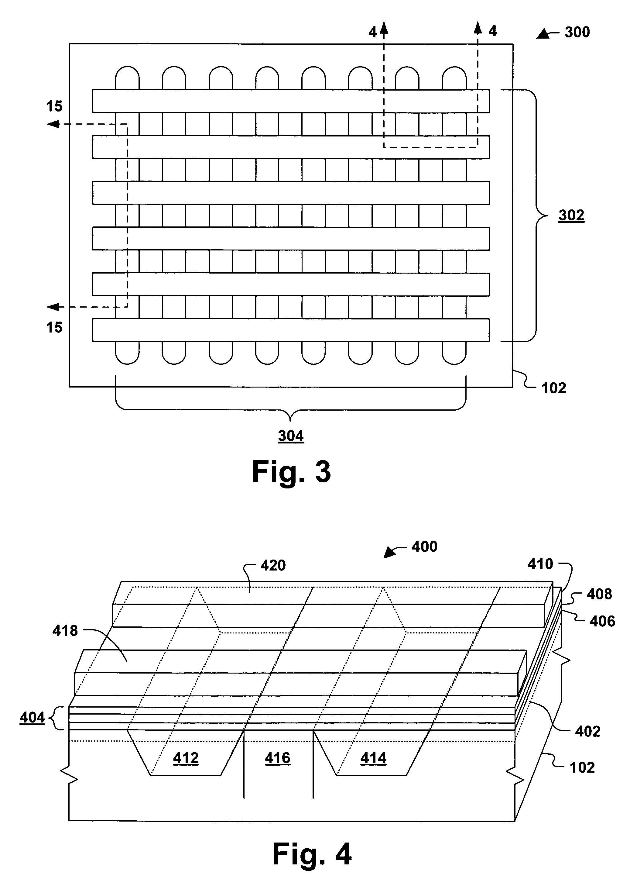
[0032]One trend in flash memory devices, particularly dual bit flash memory devices, is to increase array sizes larger and larger and to ever increasing higher densities. As a result, the amount of resistance ...


PUM


Abstract

The present invention determines or identifies programming variations for different groups within an array or memory device that properly program memory cells within the respective groups. Then, during programming operations for a given memory cell, programming voltages are applied according to the determined or identified programming variations for the group to which the given memory cell belongs. These adjusted programming variations facilitate successful programming of the particular memory cell.

Description

REFERENCE TO RELATED APPLICATION[0001]This application is a divisional application of U.S. patent application Ser. No. 10 / 860,450, U.S. Pat. No. 7,009,887, which was filed Jun. 3, 2004, entitled METHOD OF DETERMINING VOLTAGE COMPENSATION FOR FLASH MEMORY DEVICES.FIELD OF INVENTION[0002]The present invention relates generally to memory devices and the like, and in particular to determining and utilizing voltage compensation for programming of flash memory devices.BACKGROUND OF THE INVENTION[0003]Many different types and styles of memory exist to store data for computers and similar type systems. For example, random access memory (RAM), dynamic random access memory (DRAM), static random access memory (SRAM), read only memory (ROM), programmable read only memory (PROM), electrically programmable read only memory (EPROM), electrically erasable programmable read only memory (EEPROM) and flash memory are all presently available to accommodate data storage.[0004]Each type of memory has its...

Claims


Application Information

Patent Timeline
Patent Type & Authority Patents(United States)
IPC IPC(8): G11C16/04G11C16/06
CPCG11C16/12G11C29/021G11C29/028G11C29/50004G11C16/04
Inventor HSIA, EDHAMILTON, DARLENEMADHANI, ALYKHANYU, KENNETH
Owner INFINEON TECH LLC
Why Eureka
Try Eureka