Dual conducting floating spacer metal oxide semiconductor field effect transistor (DCFS MOSFET) and method to fabricate the same

a metal oxide semiconductor and field effect technology, applied in the field of semiconductor field effect transistors, can solve the problems of widening the threshold voltage distribution and mutual threshold voltage interference, and the inability of tunneling carriers to precisely inject carriers into the nitride trap area, so as to achieve good programming and erasing properties.

Active Publication Date: 2013-04-09
FLASHSILICON
View PDF10 Cites 2 Cited by
  • Summary
  • Abstract
  • Description
  • Claims
  • Application Information

AI Technical Summary

Benefits of technology

[0009]The present invention provides a Dual Conducting Floating Spacer Metal-Oxide Semiconductor Field Effect Transistor (DCFS MOSFET) which has two floating spacers made of conducting material, surrounded by insulating dielectric materials. The two physically separated and electrically isolated conducting floating spacers store charge in a non-volatile memory (NVM) application. Since the threshold voltage of a MOSFET is determined by carrier inversion near the source junction, the stored charge in the source-side conducting floating spacer can screen the capacitively coupled electrical field between the gate and the source electrode, thereby resulting in a threshold voltage change for the MOSFET. With appropriate the source / drain regions appropriately located, the stored charge on each of the conducting floating spacers can be separately read out by interchanging the device's source and drain electrodes. Thus, for an NVM application, a DCFS MOSFET can provide twice the storage capacity by storing one or more levels of charge in each of its two separate conducting floating spacers. Furthermore, unlike a charge trap material having a distribution of trap potential depths and locations, the conducting floating spacers of a DCFS MOSFET are made of material in a well-defined geometry, thus preserving the good programming and erasing properties of a conventional conducting floating gate device. The DCFS MOSFET of the present invention may be scaled down according to conventional MOSFET scaling rules.

Problems solved by technology

Although the NROM-type NVM devices (MirrorBit™, available from Spansion) have been in production, the challenges of controlling nitride film properties and scaling down device geometry still remain.
One challenge is to fill and to remove charge from inhomogeneous nitride traps in well-controlled areas above the device channel region.
However, conventional programming methods, such as hot carrier injection (HCI), Fowler-Nordheim tunneling, and band-to-band tunneling cannot inject carriers into the nitride trap areas as precisely as desired because of programming non-uniformity and device inhomogeneity.
Such non-uniformity can lead to a wider threshold voltage distribution and mutual threshold voltage interference between the source and drain terminals during programming.
To remove stored electrons from the nitride traps using the Fowler-Nordheim tunneling mechanism requires a long erasing time and a relatively thinner, high voltage-limited nitride film, due to the adverse effect of reversed charge injection from the control gate.
In reading, such a device is known to accumulate charge in its dielectric films, so that the sub-threshold slope of the MOSFET device is degraded, thereby resulting in a larger off-leakage current.
The residual charge accumulation effect from programming and erase cycles may lead to a severe degradation in an NVM device.
These issues of the NROM NVM device is expected to worsen, as the trapped electron area has to increase to achieve a higher threshold voltage shift and the device channel length has to be shortened to scale down the device.

Method used


Image

  • Dual conducting floating spacer metal oxide semiconductor field effect transistor (DCFS MOSFET) and method to fabricate the same
  • Dual conducting floating spacer metal oxide semiconductor field effect transistor (DCFS MOSFET) and method to fabricate the same
  • Dual conducting floating spacer metal oxide semiconductor field effect transistor (DCFS MOSFET) and method to fabricate the same

Examples


Embodiment Construction

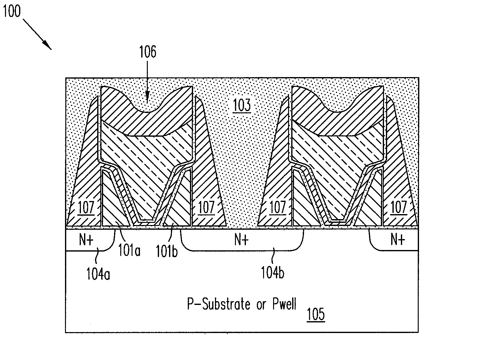
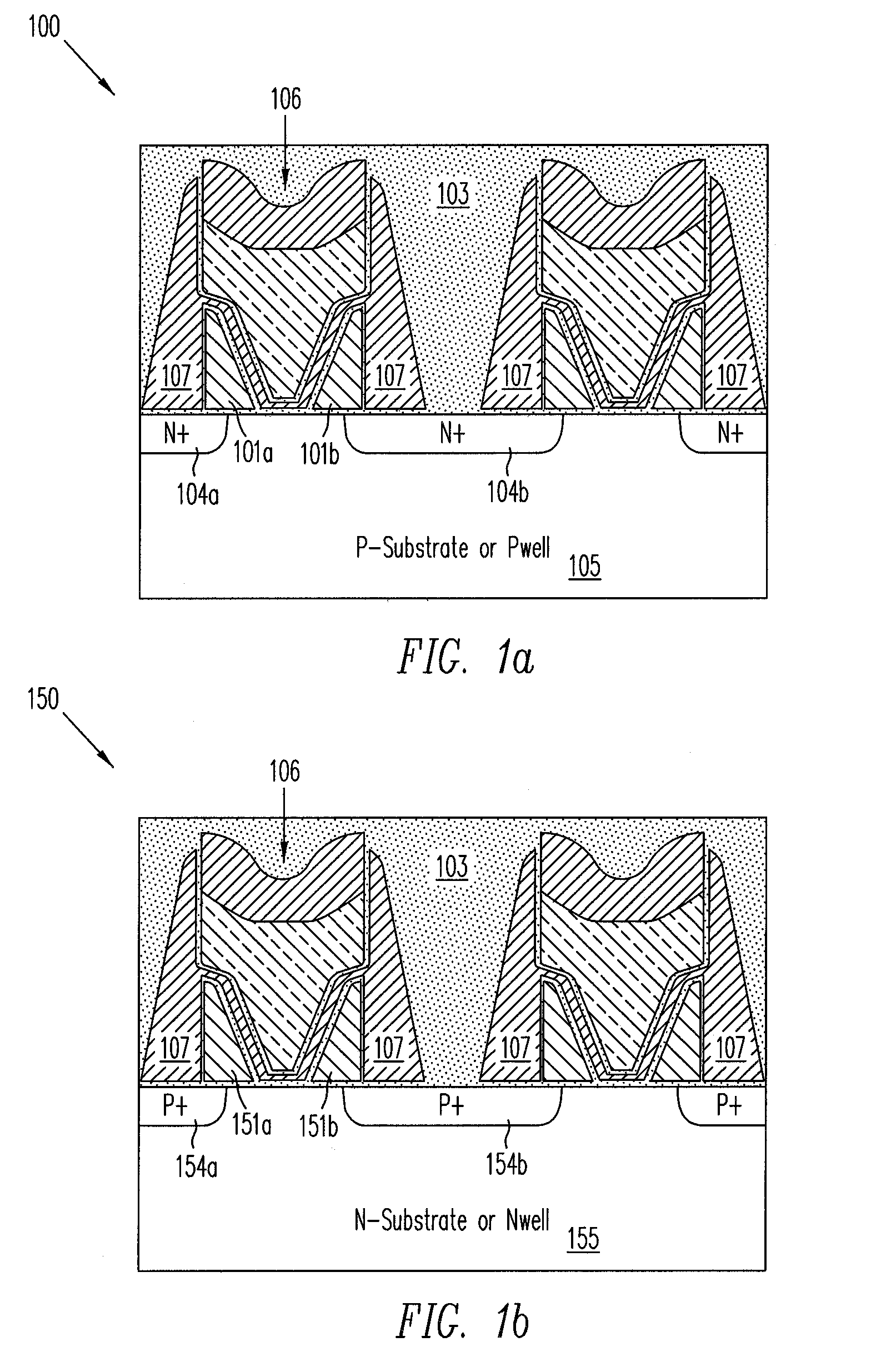
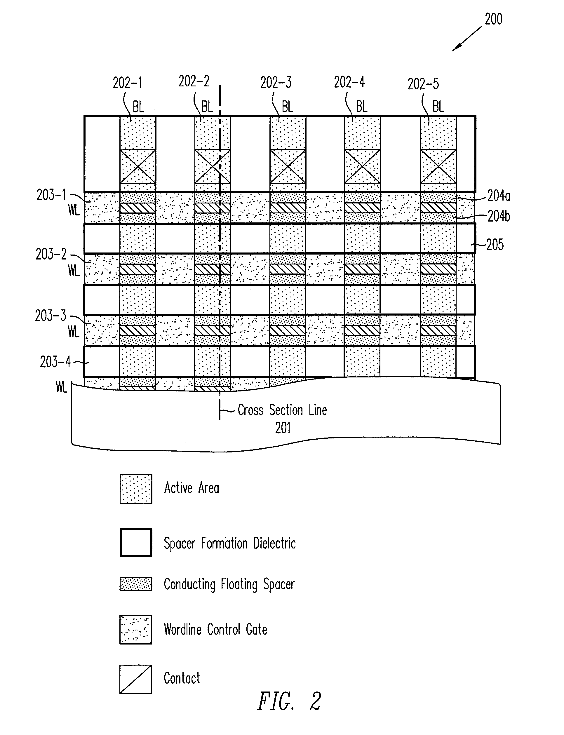
[0021]FIGS. 1(a) and 1(b) show cross-sections of dual conducting floating spacer NVM devices, for N-channel and P-channel devices, respectively, in NAND-type flash arrays, according to one embodiment of the present invention. FIG. 2 is a layout view of NAND-type array 200 of DCFS devices, such as those shown in FIG. 1(a) or FIG. 1(b), in accordance with one embodiment of the present invention. The cross-sections of FIG. 1(a) and FIG. 1(b) may be seen from the cross section line 201, depending on whether N-channel or P-channel devices are fabricated.

[0022]As shown in FIG. 1(a), conducting floating spacers 101a and 101b are made of conducting material residing on each side of MOSFET 100, surrounded by dielectric material 103. Charge may be stored in each of conducting floating spacers 101a and 101b, which slightly overlap source / drain electrode diffusion regions 104a and 104b on the sides of MOSFET 100. The two junctions located below floating spacers 101a and 101b are formed by heavy...


PUM


Abstract

Dual Conducting Floating Spacer Metal Oxide Semiconductor Field Effect Transistors (DCFS MOSFETs) and methods for fabricate them using a process that is compatible with forming conventional MOSFETs are disclosed. A DCFS MOSFET can provide multi-bit storage in a single Non-Volatile Memory (NVM) memory cell. Like a typical MOSFET, a DCFS MOSFET includes a control gate electrode on top of a gate dielectric-silicon substrate, thereby forming a main channel of the device. Two electrically isolated conductor spacers are provided on both sides of the control gate and partially overlap two source / drain diffusion areas, which are doped to an opposite type to the conductivity type of the substrate semiconductor. The DCFS MOSFET becomes conducting when a voltage that exceeds a threshold is applied at the control gate and is coupled through the corresponding conducting floating spacer to generate an electrical field strong enough to invert the carriers near the source junction. By storing charge in the two independent conducting floating spacers, DCFS MOSFET can have two independent sets of threshold voltages associated with the source junctions.

Description

BACKGROUND OF THE INVENTION[0001]1. Field of the Invention[0002]The present invention relates to semiconductor devices. More specifically, the present invention relates to fabricating Dual Conducting Floating Spacer Metal-Oxide-Semiconductor Field Effect Transistors (DCFS MOSFETs) using a process that is compatible with manufacturing conventional MOSFETs on the same wafer.[0003]2. Discussion of the Related Art[0004]Semiconductor non-volatile memory (NVM) and, particularly, electrically-erasable, programmable read-only memories (EEPROMs) are used in a wide range of electronic equipment (e.g., computers, telecommunications hardware and consumer appliances). In general, EEPROMs are often used to store firmware and data, as the content is maintained even with power off and may be altered as needed. The flash EEPROM may be regarded as a specially configured EEPROM that may be erased only on a global or sector-by-sector basis. The application of flash memory as a mass code and data storag...

Claims


Application Information

Patent Timeline
Patent Type & Authority Patents(United States)
IPC IPC(8): H01L29/788
CPCH01L21/28273H01L27/11521H01L29/7887H01L29/66825H01L29/42332H01L29/40114H10B41/30
Inventor WANG, LEE
Owner FLASHSILICON
Why Eureka
Try Eureka