Test reading apparatus for memories

a memory and test reading technology, applied in the field of test reading apparatus, can solve the problems of increasing test time, affecting the total production time and hence the cost, and achieve the effect of shortening the test tim

Active Publication Date: 2007-02-27
INFINEON TECH AG
View PDF24 Cites 2 Cited by
  • Summary
  • Abstract
  • Description
  • Claims
  • Application Information

AI Technical Summary

Benefits of technology

[0006]It is an object of the present invention to provide an arrangement which permits a shorter test time.
[0007]It contains a test reading apparatus having a memory device having individual memory cells and having a buffer device which is connected to the memory device and which stores data written to the memory cells in the memory device. The test reading apparatus also contains an apparatus, which has an input and an output, and at least one test reference source which is switchably coupled to the input of the apparatus by data stored in the buffer device. The test reading apparatus contains a test apparatus which is connected to the buffer device and to the output of the apparatus and which is designed to compare a signal at the output of the apparatus with data stored in the buffer device.
[0008]The buffer device is therefore able to select the at least one test reference source which corresponds to the logic state for the memory array's memory cell which is under test. The weighting operation in the test apparatus is always performed with the correct value of the test reference signal. It is thus possible to dispense with a fresh read operation.
[0009]A method for test reading stored logic states in a memory device produces a test signal which is dependent on the nominal value of the logic state. This test signal is compared with the logic state which is under test. Since a test signal is always produced for each logic state which under test, said test signal being used to assess whether the state under test is correct, one read operation for all of the memory device's states under test is sufficient. It goes without saying that each logic state under test for the memory device is stored in a memory cell in the memory device.
[0010]It is thus advantageous if the apparatus has a sense amplifier. In one development of the invention, the memory device is in the form of a rewritable read only memory or a nonvolatile memory. It can thus be used particularly for use in chip cards. The buffer device is used in an advantageous development for programming the memory device.
[0011]One advantageous refinement is for the test reference source to be in the form of two reference signal sources. The signals from the two test reference sources each correspond to a logic state. For this reason, the content of the buffer device can be taken as a basis of respectively connecting a test reference source to an input on the sense amplifier.

Problems solved by technology

This results in an increased test time, which has disadvantageous effects on the total production time and hence the costs, particularly during mass production, for example in chip cards.

Method used


Image

  • Test reading apparatus for memories
  • Test reading apparatus for memories
  • Test reading apparatus for memories

Examples


Embodiment Construction

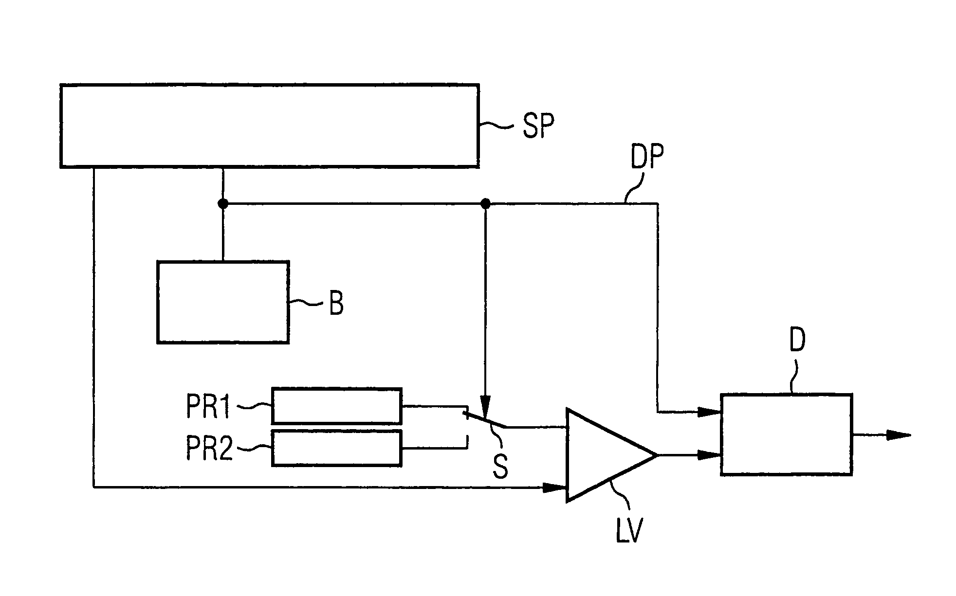
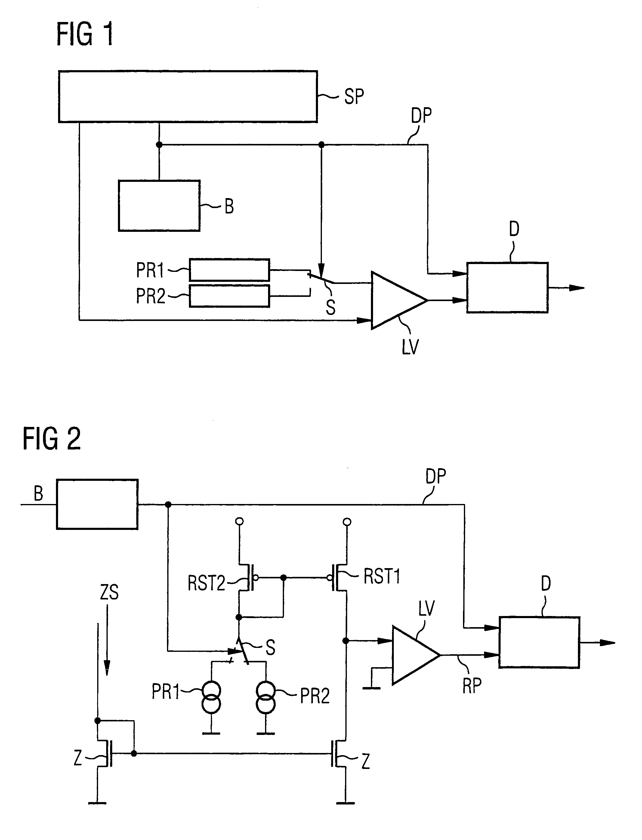
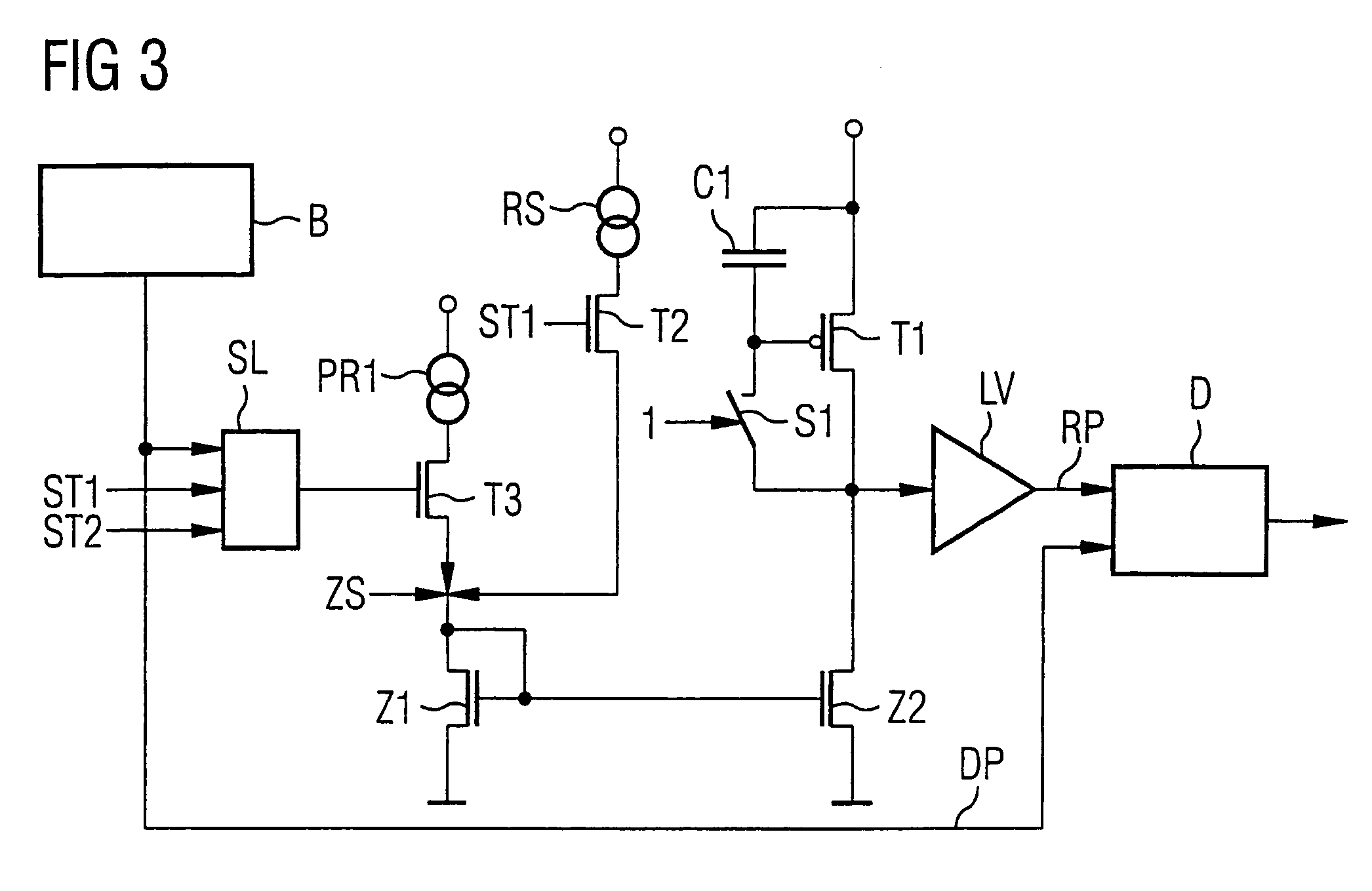
[0019]FIG. 1 shows a test reading apparatus which is part of a chip (not shown in more detail) in a chip card. The test reading apparatus has a memory device SP which contains a plurality of individual memory cells (not shown here). The individual memory cells in the memory device SP contain a respective one of two logic states in line with their programming.

[0020]The data in the memory device SP which correspond to the content of the individual memory cells are likewise stored in the buffer device B, which is connected to the memory device SP. The memory device SP is also coupled to a sense amplifier LV which is in the form of an operational amplifier. A second input on the sense amplifier LV is connected to a switch S which can connect two test reference sources PR1 and PR2 to the second input of the sense amplifier.

[0021]The output of the sense amplifier LV is connected to the input of a test device D. The second input of the test device D is coupled to the buffer device B via DP...


PUM


Abstract

Test reading apparatus having a memory device having individual memory cells, a buffer device, which is connected to the memory device, and which stores data written to the memory cells in the memory device, an apparatus which has an input and an output, at least one test reference source which can be connected to the input of the apparatus by data stored in the buffer device, and a test apparatus, which is connected to the buffer device and to the output of the apparatus, and which is designed to compare a signal at the output of the apparatus with data stored in the buffer device.

Description

CROSS-REFERENCE TO RELATED APPLICATION[0001]This application claims priority to German Patent Application No. 10327284.4, which was filed Jun. 17, 2003, and is incorporated herein by reference in its entirety.FIELD OF THE INVENTION[0002]The invention relates to a test reading apparatus for test reading a memory device when the memory has been programmed. The invention also relates to a method for test reading stored logic states in a memory device.BACKGROUND OF THE INVENTION[0003]When nonvolatile read only memories have been programmed, the data stored in the memory are checked. To this end, the data are read again using more stringent criteria than during a later, normal read operation. As an example of this, mention will be made of the read operation in a memory in which the current in a memory cell which is being read in the memory is compared with a reference current. A different reference current is used for a check.[0004]Test reading involves the contents of the individual mem...

Claims


Application Information

Patent Timeline
Patent Type & Authority Patents(United States)
IPC IPC(8): G11C29/00G11C16/34
CPCG11C16/3459G11C16/3454
Inventor DIRSCHERL, GERDSEDLAK, HOLGERSCHLAGER, TOBIAS
Owner INFINEON TECH AG
Why Eureka
Try Eureka