
Method for processing IC designs for different metal BEOL processes

a technology of metal beol and processing method, which is applied in the field of semiconductor devices, can solve the problems of only being able to utilize the al process, no longer desirable or even practical to continue to invest in al process, and immediate applicability of complex wiring

Inactive Publication Date: 2008-10-28
CHARTERED SEMICONDUCTOR MANUFACTURING
View PDF15 Cites 17 Cited by
  • Summary
  • Abstract
  • Description
  • Claims
  • Application Information

AI Technical Summary

Problems solved by technology

The complexity of this wiring becomes immediately appreciable once one realizes that there are usually hundreds of millions or more semiconductor devices (transistors in particular) formed on a single IC, and all these semiconductor devices need to be properly connected.
Microchip interconnect technology has become a critical challenge for future IC advancements due to the increasing difficulties to reduce signal propagation delay or interference caused by the increasingly dense interconnects.
The problem is particularly acute considering that while an increase of metallization density means longer signal delays caused by the interconnects, a corresponding increase of transistor density means shorter signal traveling time between local semiconductor devices, making metallization increasingly a bottleneck in enhancing IC performance.
With Cu technology becoming more mature, continue to invest in Al process is no longer desirable or even practical since it will add tremendous overhead to operations and facility managements.
In addition, Al process can only be utilized up to 0.15 μm and clearly has a limited service life span, making further investments by chipmakers in the desolating technology more difficult.
This led to an undesirable situation where a company that has a product design based on Al process will have to either redesign the product for Cu process or find a chipmaker who still maintains a production line based on Al technology, which is becoming increasingly more difficult or less economical.

Method used


Image

  • Method for processing IC designs for different metal BEOL processes
  • Method for processing IC designs for different metal BEOL processes
  • Method for processing IC designs for different metal BEOL processes

Examples


Embodiment Construction

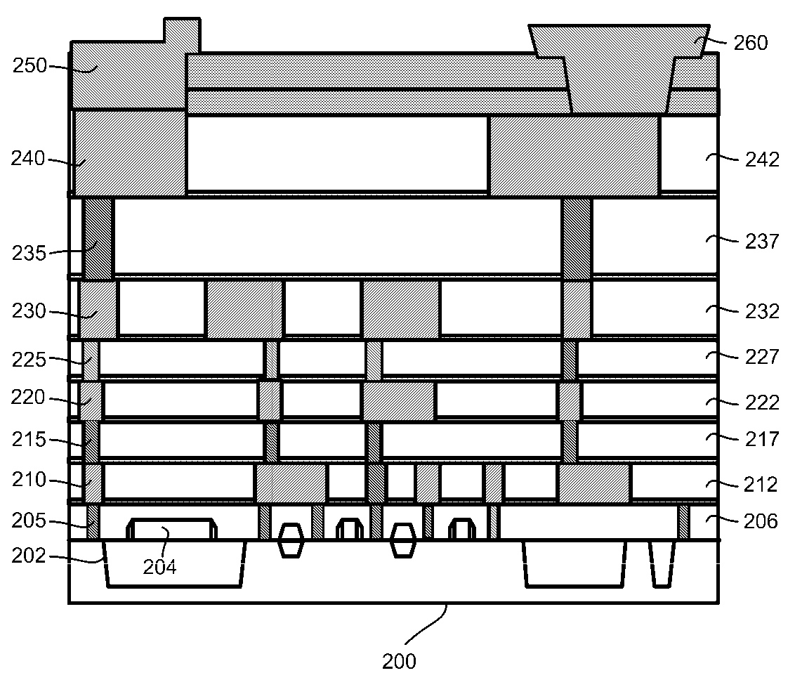
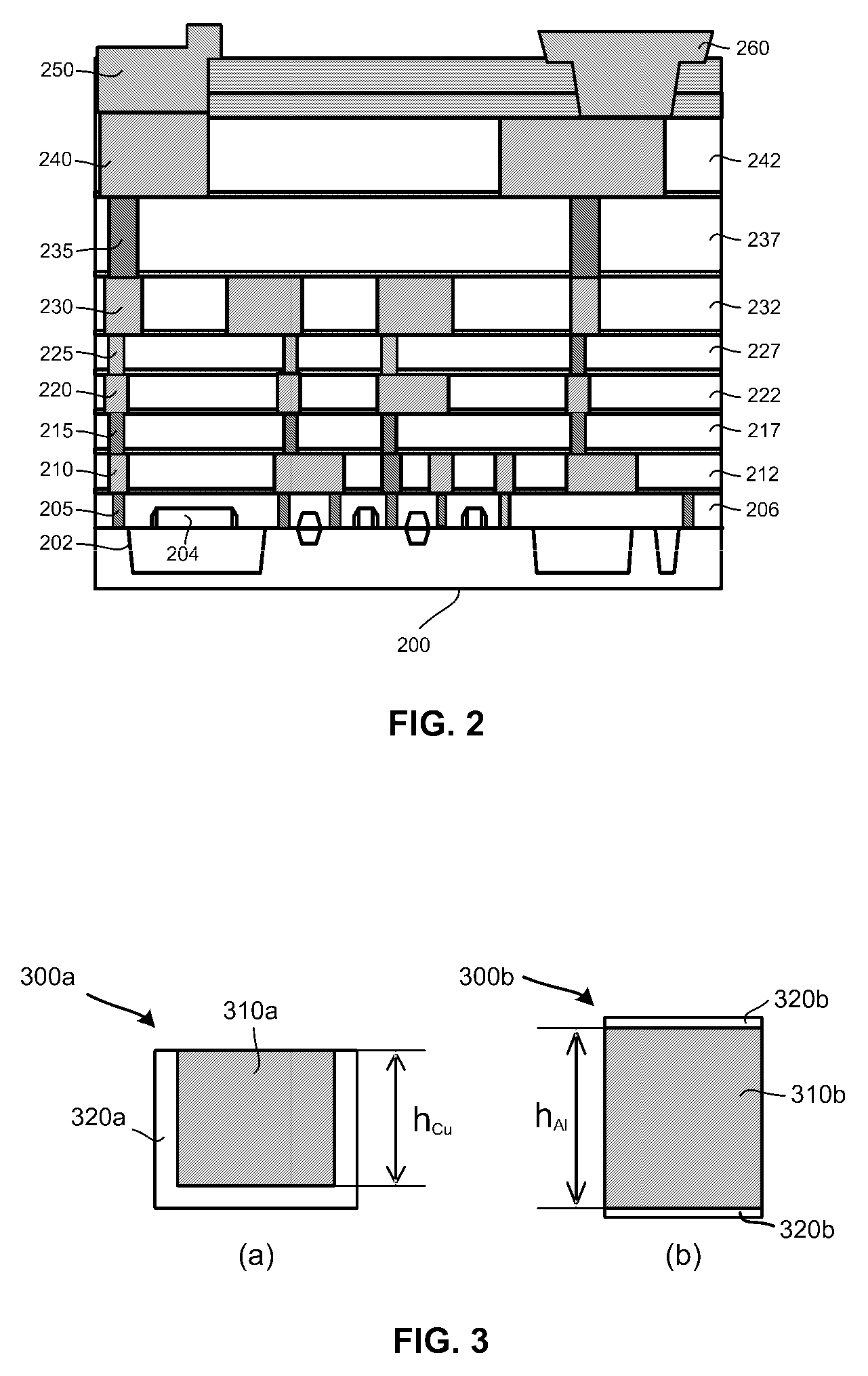
[0029]Disclosed below are representative embodiments of a method of processing IC designs for different metal BEOL processes. The representative embodiments are disclosed herein for purposes of illustrating. The disclosed systems and methods should not be construed as limiting in any way. Instead, the present disclosure is directed toward all novel and nonobvious features and aspects of the various disclosed embodiments, alone and in various combinations and subcombinations with one another. Therefore, these and other variations upon the specific embodiments are intended to be covered by the present inventions. The systems and methods are not limited to any specific aspect or feature or combinations thereof, nor to the disclosed systems and methods require that any one or more specific advantages be present or problems be solved.

[0030]In the present disclosure, the terms “BEOL fabrication process,”“BEOL process,”“backend fabrication process,”“backend process,” and “backend technolog...


PUM

PropertyMeasurementUnit
dielectric constantaaaaaaaaaa

Abstract

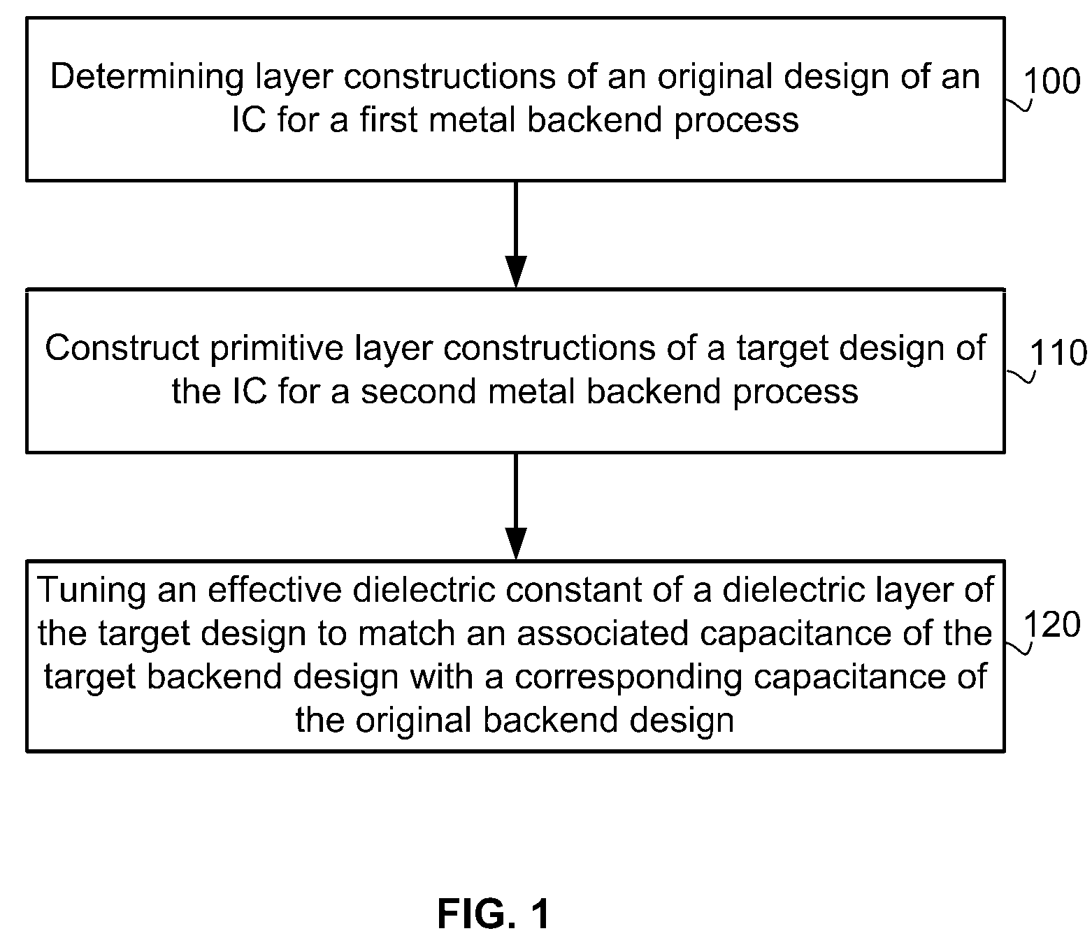
A method for processing IC designs for different metal BEOL processes is provided for enabling fabricating using a metal fabrication process an IC originally having a backend design for a different metal fabrication process. The method first determines layer constructions of an original design of an IC for a first metal backend process, and, based on the layer constructions of the original design of the IC, constructs primitive layer constructions of a target design of the IC for a second metal backend process. The method then tunes an effective dielectric constant of a dielectric layer of the target design to match an associated capacitance of the target backend design with a corresponding capacitance of the original backend design. The method can be used to convert a backend design of an IC from an old metal process (such as Al process) to a new metal process (such as Cu process), without redesigning the IC for the new metal BEOL fabrication process.

Description

CROSS-REFERENCE TO RELATED APPLICATIONS[0001]The present application is related to commonly assigned U.S. patent application, entitled “A Method for Using a Cu BEOL Process to Fabricate an Integrated Circuit (IC) Originally Having an Al Design”, filed on even date.BACKGROUND[0002]1. Field of the Invention[0003]The present invention relates generally to the field of semiconductors, particularly to manufacturing methods for fabricating semiconductor devices, and more particularly to the Back-End-Of-Line (BEOL) semiconductor manufacturing process.[0004]2. Description of the Prior Art[0005]The semiconductor manufacturing process, when likened to an assembly line, includes two major components, namely the Front-End-of-Line (FEOL) which includes the multilayer process of the actual forming of semiconductor devices (transistors, etc.) on a semiconductor substrate, and the Back-End-Of-Line (BEOL) which includes the metallization after the semiconductor devices have been formed. Like all ele...

Claims


Application Information

Patent Timeline
Patent Type & Authority Patents(United States)
IPC IPC(8): H01L21/4763
CPCH01L23/5222H01L23/5283H01L23/53238H01L23/53295H01L2924/0002H01L2924/00
Inventor SU, JIANNONGYANG, SIMON SHI-NINGZHANG, JIAN
Owner CHARTERED SEMICONDUCTOR MANUFACTURING
Learn More