
Method for driving in-plane switching mode liquid crystal display device

a liquid crystal display and in-plane switching technology, applied in the direction of electric digital data processing, instruments, computing, etc., can solve the problems of difficult to obtain difficult to achieve a wide viewing angle, and the frame inversion method is sensitive to flicker generation, so as to achieve the effect of increasing the liquid crystal voltag

Inactive Publication Date: 2008-10-28
LG DISPLAY CO LTD
View PDF2 Cites 14 Cited by
  • Summary
  • Abstract
  • Description
  • Claims
  • Application Information

AI Technical Summary

Benefits of technology

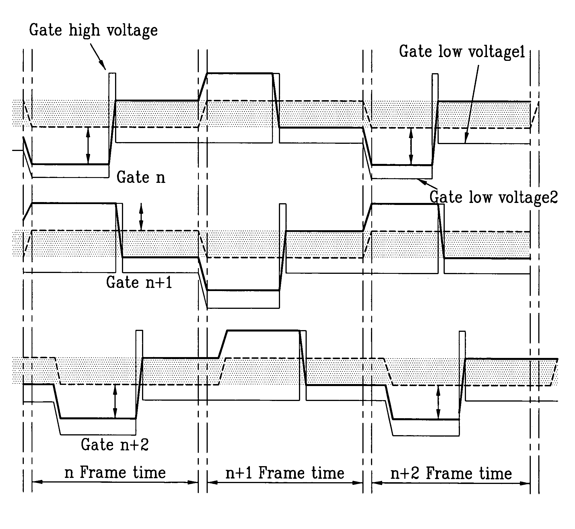
The invention is about an improved method for driving an IPS mode LCD device that solves problems associated with current technology. The method involves applying a common voltage to each common line in a state where thin film transistors are alternately positioned at lower and upper side pixel regions adjacent to the corresponding gate line, and common lines are formed in a zigzag-type configuration along the thin film transistors in the pixel regions. This method increases the liquid crystal voltage between a common electrode and a pixel electrode without using a high-power source driver, and prevents leakage current by swing of the common voltage. The invention also includes a method for driving an In-Plane switching (IPS) mode LCD device that includes multiple gate and data lines, thin film transistors, and common lines in a zigzag-type configuration along the thin film transistors in the pixel regions. The common voltage is applied so that a first common voltage or a second common voltage is inversely applied to even numbered common lines or odd numbered common lines in one vertical period for being synchronized with a scanning signal supplied to the first gate line, and a gate Low voltage applied to each gate line is lower than a pixel voltage. The invention also includes a method for driving an In-Plane switching (IPS) mode LCD device that includes first and second substrates being opposite to each other, and a liquid crystal material layer between the first and second substrates. The thin film transistors are formed over the first substrate in a matrix configuration.

Problems solved by technology

Despite various technical developments in the LCD technology for applications in different fields, research in enhancing the picture quality of the LCD device has been, in some respects, lacking as compared to other features and advantages of the LCD device.
Thus, it is difficult to obtain a wide viewing angle.
However, the frame inversion method is sensitive to flicker generated according to an asymmetrical transmittance between the positive and negative polarities.
In addition, the frame inversion method is susceptible to crosstalk caused by interference between data signals of adjacent pixels.
However, the polarity of the data voltage is the same along a horizontal direction, so that horizontal crosstalk is generated, and consumption current increases due to an increase of the number of switching operations, as compared with that during the frame inversion.
However, the dot inversion method is problematic since the dot inversion method uses a high-voltage driver that results in a high consumption current.
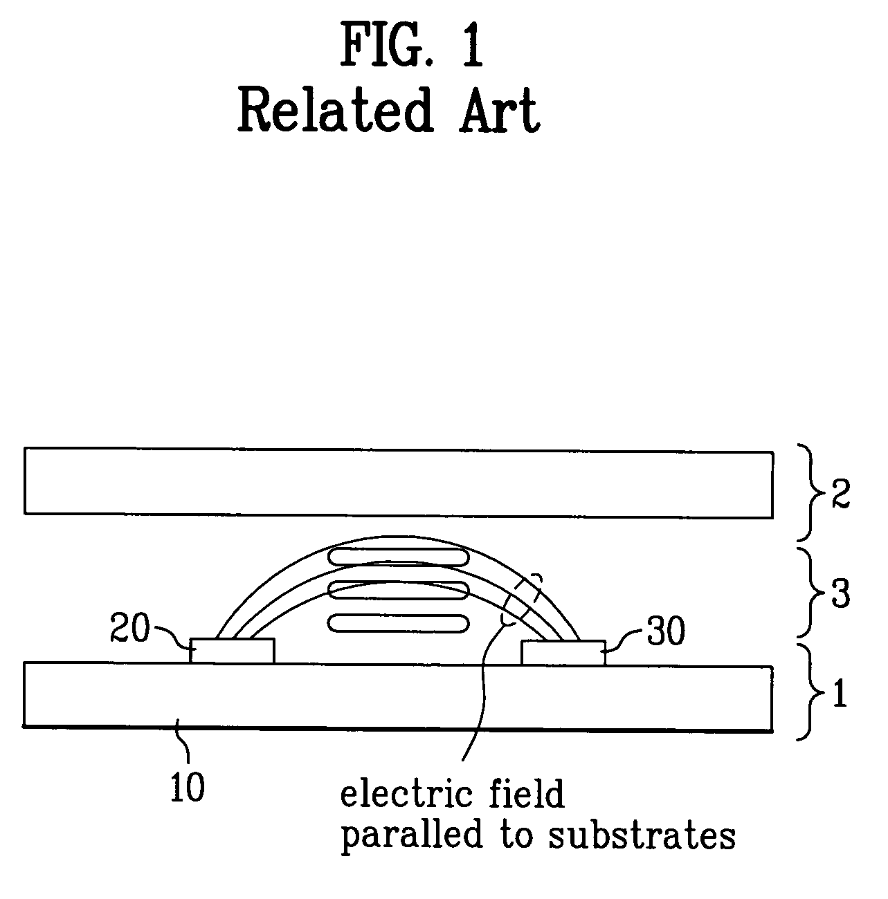
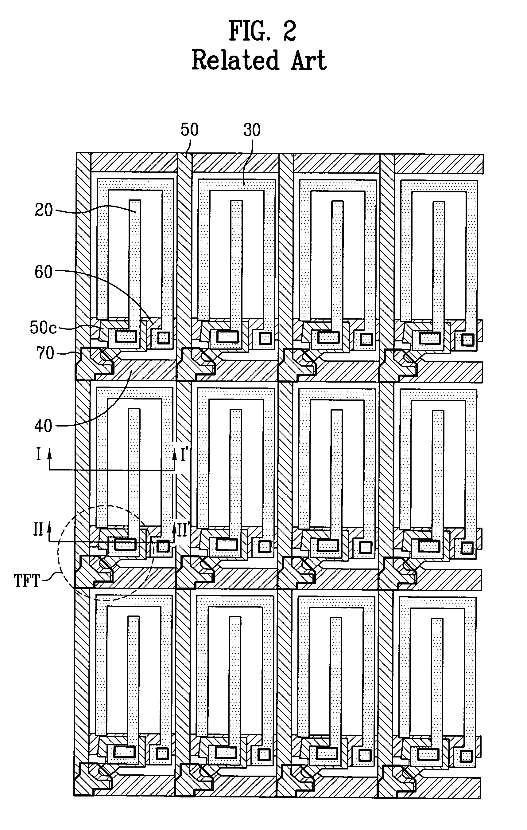
However, the related art IPS mode LCD device has many disadvantages, some of which are described below.
However, since a source driver having a high output value is expensive, it has been necessary to obtain low power consumption by lowering the output value to thereby decrease manufacturing costs.
However, if the interval between the pixel electrode and the common electrode becomes narrow, then the aperture ratio of the pixel deteriorates.
However, patterns having various shapes are formed within the pixel region so that it is difficult to uniformly transmit the light.

Method used


Image

  • Method for driving in-plane switching mode liquid crystal display device
  • Method for driving in-plane switching mode liquid crystal display device
  • Method for driving in-plane switching mode liquid crystal display device

Examples


Embodiment Construction

[0064]Reference will now be made in detail to the preferred embodiments of the invention, examples of which are illustrated in the accompanying drawings. Wherever possible, the same reference numbers will be used throughout the drawings to refer to the same or like parts.

[0065]Hereinafter, an In-Plane switching (IPS) mode liquid crystal display (LCD) device according to the invention will be described with reference to the accompanying drawings.

[0066]FIG. 10 shows a layout illustrating a pixel structure of an IPS mode LCD device according to a first embodiment of the invention. FIG. 11 shows a cross-sectional view taken along line III-III′ of FIG. 10. FIG. 12 shows a cross-sectional view taken along line IV-IV′ of FIG. 10. As shown in FIG. 10 to FIG. 12, the IPS mode LCD device according to the first embodiment of the invention includes multiple gate and data lines 210 and 220, multiple thin film transistors TFTs, multiple pixel electrodes 230, multiple common (storage) lines 250, a...


PUM

PropertyMeasurementUnit
viewing angleaaaaaaaaaa
constant voltageaaaaaaaaaa
voltageaaaaaaaaaa

Abstract

A method for driving an IPS mode LCD device prevents leakage current by swing of a common voltage. The IPS mode LCD device includes multiple gate and data lines crossing each other to define a plurality of pixel regions, multiple thin film transistors (TFT) alternately positioned at lower and upper side pixel regions adjacent to the corresponding gate line, and multiple common lines in a zigzag type along the thin film transistors in the pixel regions. A common voltage is applied so that a first common voltage or a second common voltage is inversely applied to even numbered common lines or odd numbered common lines in one vertical period to be synchronized with a scanning signal supplied to the first gate line, and a gate Low voltage applied to each gate line is lower than a pixel voltage on transition of the common voltage from “High” to “Low”.

Description

[0001]This application claims the benefit of Korean Application No. P2003-44921, filed on Jul. 3, 2003, which is hereby incorporated by reference.BACKGROUND OF THE INVENTION[0002]1. Field of the Invention[0003]The invention pertains to an In-Plane switching (IPS) mode liquid crystal display (LCD) device, and more particularly, to a method for driving an IPS mode LCD device, to prevent a leakage current by a common voltage swing.[0004]2. Discussion of the Related Art[0005]Demand for various display devices have increased with the development of an information society. Accordingly, many efforts have been made to research and develop various flat display devices such as a liquid crystal display (LCD), a plasma display panel (PDP), an electroluminescent display (ELD), and a vacuum fluorescent display (VFD). Some types of flat display devices have already been utilized as displays for various types of equipment.[0006]Among the various flat display devices, liquid crystal display (LCD) de...

Claims


Application Information

Patent Timeline
Patent Type & Authority Patents(United States)
IPC IPC(8): G09G3/36G02F1/133G02F1/1343
CPCG02F1/134363G09G3/3655G09G3/3614G09G2300/0434G09G2310/06G09G2320/0214G02F1/133
Inventor LEE, JAE KYUNKIM, KYONG SOEK
Owner LG DISPLAY CO LTD
Learn More