Connector housing block, interface member and electronic device testing apparatus

a technology of connector housing and interface member, which is applied in the direction of coupling device connection, electric discharge lamp, instruments, etc., can solve the problems of increasing production cost, increasing the number of parts, and affecting the quality of the product, so as to reduce the number of parts of the connector housing, improve the mounting density of the connector pin, and reduce the number of parts

Inactive Publication Date: 2008-12-02
ADVANTEST CORP
View PDF21 Cites 33 Cited by
  • Summary
  • Abstract
  • Description
  • Claims
  • Application Information

AI Technical Summary

Benefits of technology

[0027]According to the present invention, it is possible to reduce the number of parts of the connector housing, and mounting density of the connector pins can be improved, that is, the connector pins can be arranged at high density. Also, by attaching the connector housing in a floating state, a positional error can be absorbed when fitting the connector housing.

Problems solved by technology

Connector pins provided to the interface member are connected to connector pins of the performance board and, when fitting the connectors of the interface member with the connectors of the performance board to attach the performance board to the interface member, positional error may arise between the both connectors.
However, when each of the connector pins 242P is made separately movable by the floating structure by the coil spring 246P, there are disadvantages that the number of parts increases and the production cost increases.
However, when providing the coil springs 246P to the respective connector pins 242P, the connector pins 242P cannot be arranged close to each other and hard to be mounted at high density.
Also, due to the limitation of the mounting density of the connector pins 242P, there is a disadvantage that the interface member becomes large.

Method used


Image

  • Connector housing block, interface member and electronic device testing apparatus
  • Connector housing block, interface member and electronic device testing apparatus
  • Connector housing block, interface member and electronic device testing apparatus

Examples


Embodiment Construction

[0052]Below, an embodiment of the present invention will be explained based on the drawings.

[0053]An electronic device testing apparatus in the present embodiment comprises a test head 1 shown in FIG. 1 and a not shown handler and tester. The handler is for handling an IC device 10 (an example of an electronic device) and mounting on the test head 1, and the tester is for generating an electronic signal and sending / receiving the electronic signal to / from the test head 1.

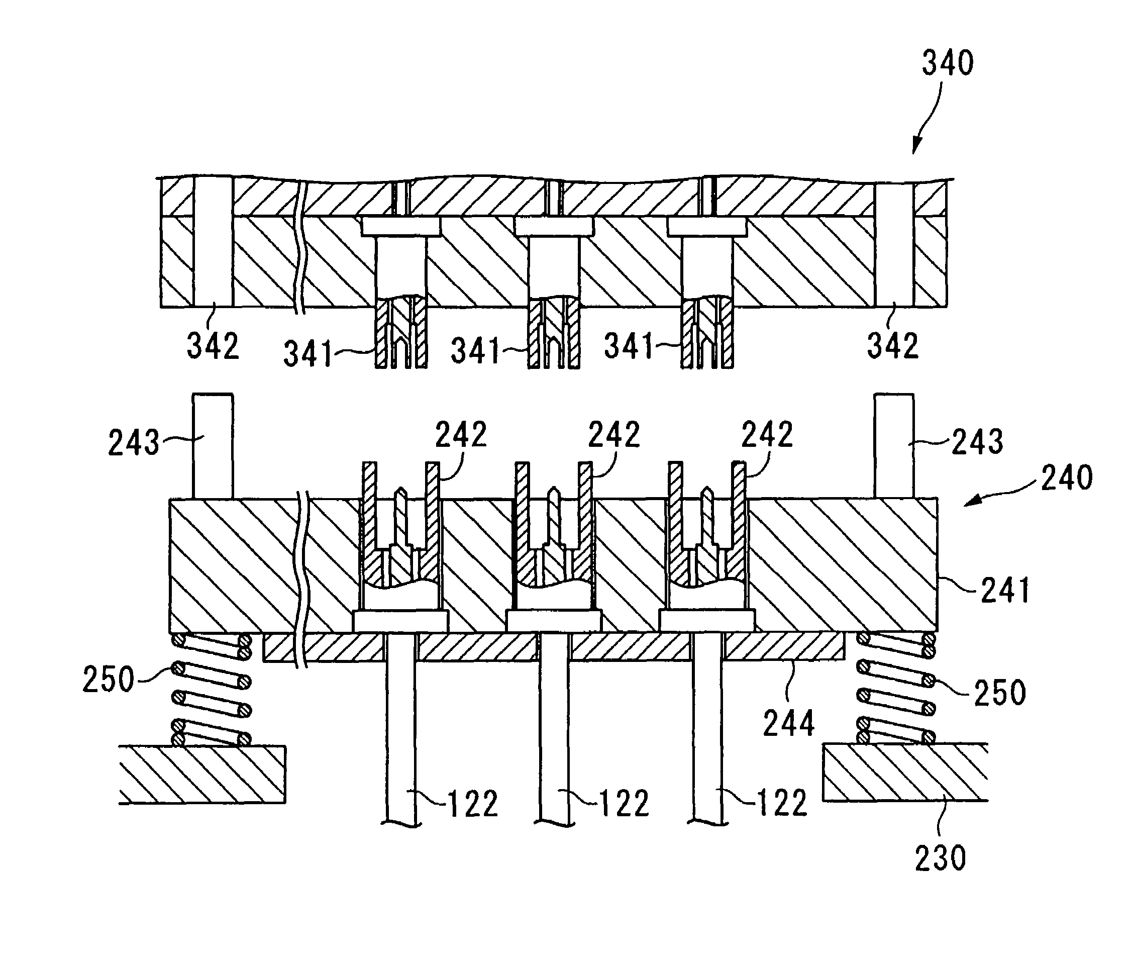
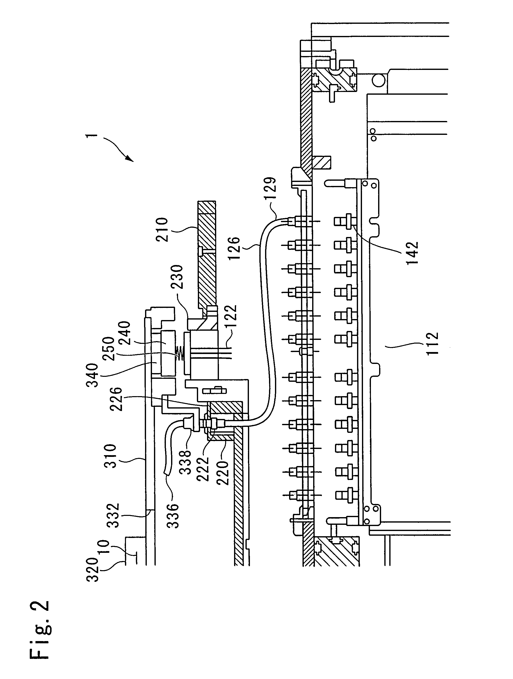
[0054]The test head 1 comprises, as shown in FIG. 1, a test head body 100 for inputting / outputting a test signal, a performance board 300 for IC devices 10 to be detachably attached, and an interface member 200 for electrically connecting the test head body 100 with the performance board 300. Note that the performance board 300 is also called, for example, as a load board or a circuit board, and the interface member 200 is also called, for example, as a hi-fix, a test head chassis, a test fixture or top plate.

[0055]A...


PUM


Abstract

In a connector housing block 260 comprising an interface member 200 for electrically connecting a test head body 100 with sockets 320 in an electronic device testing apparatus, a connector housing 240 provided with a plurality of connector pins 242 in a non-floating state is attached to a block base 230 in a floating state via a coil spring 250. Due to the configuration, the number of parts of the connector housing 240 can be reduced, mounting density of the connector pins 242 can be improved, and a positional error of the connector housing 240 can be absorbed.

Description

CROSS REFERENCE TO RELATED APPLICATIONS[0001]This application is a continuation of PCT / JP2006 / 300338, filed on Jan. 13, 2006, the contents of which are incorporated herein by reference.TECHNICAL FIELD[0002]The present invention relates to a connector housing block used for an interface for electrically connecting a test head body with sockets in an electronic device testing apparatus, and an interface member and electronic device testing apparatus provided with the connector housing block.BACKGOUND ART[0003]Conventionally, as an electronic device testing apparatus for testing performance and function of IC device and other electronic device, those including a test head body incorporating a signal module for processing signals, a performance board provided with sockets for an electronic device to be detachably attached, and an interface member provided between the signal module of the test head and the performance board for connecting the two are known.[0004]In an electronic device t...

Claims


Application Information

Patent Timeline
Patent Type & Authority Patents(United States)
IPC IPC(8): G01R31/02
CPCG01R1/0416H01R13/6315G01R31/2889H01R13/748H01R2201/20
Inventor MINEO, HIROYUKI
Owner ADVANTEST CORP
Why Eureka
Try Eureka