Carbon nanotube device fabrication

a carbon nanotube and device technology, applied in the field of carbon nanotube synthesis, can solve the problem that the nanotube cannot meet the commercial manufacturing requirements, and achieve the effect of a wide range of applications

Inactive Publication Date: 2008-12-16
PRESIDENT & FELLOWS OF HARVARD COLLEGE
View PDF42 Cites 32 Cited by
  • Summary
  • Abstract
  • Description
  • Claims
  • Application Information

AI Technical Summary

Problems solved by technology

Without such control, nanotubes cannot meet the commercial manufacturing requirements of applications for which nanotubes are so well suited.

Method used


Image

  • Carbon nanotube device fabrication
  • Carbon nanotube device fabrication
  • Carbon nanotube device fabrication

Examples


example

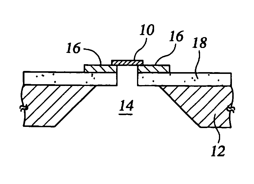
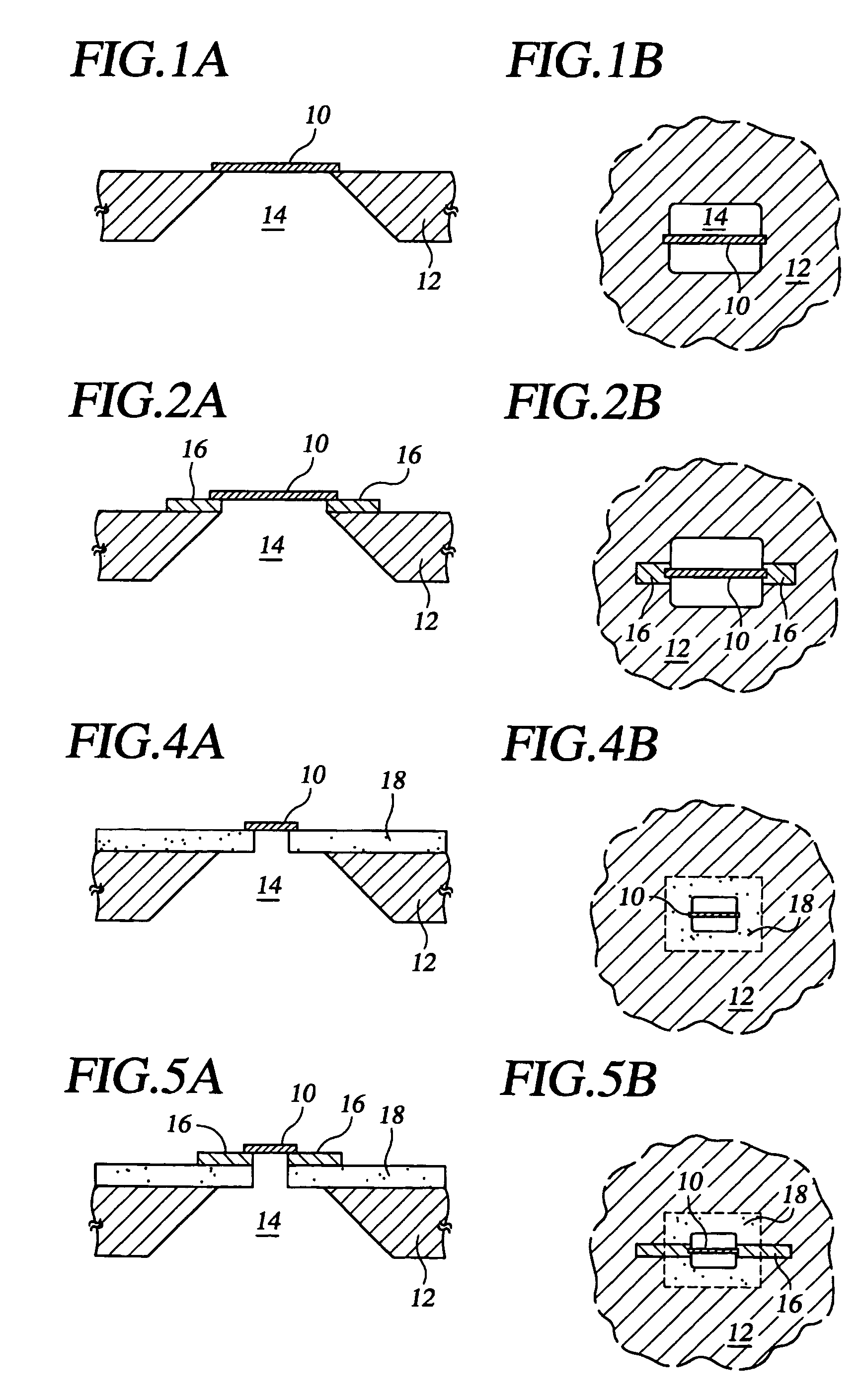
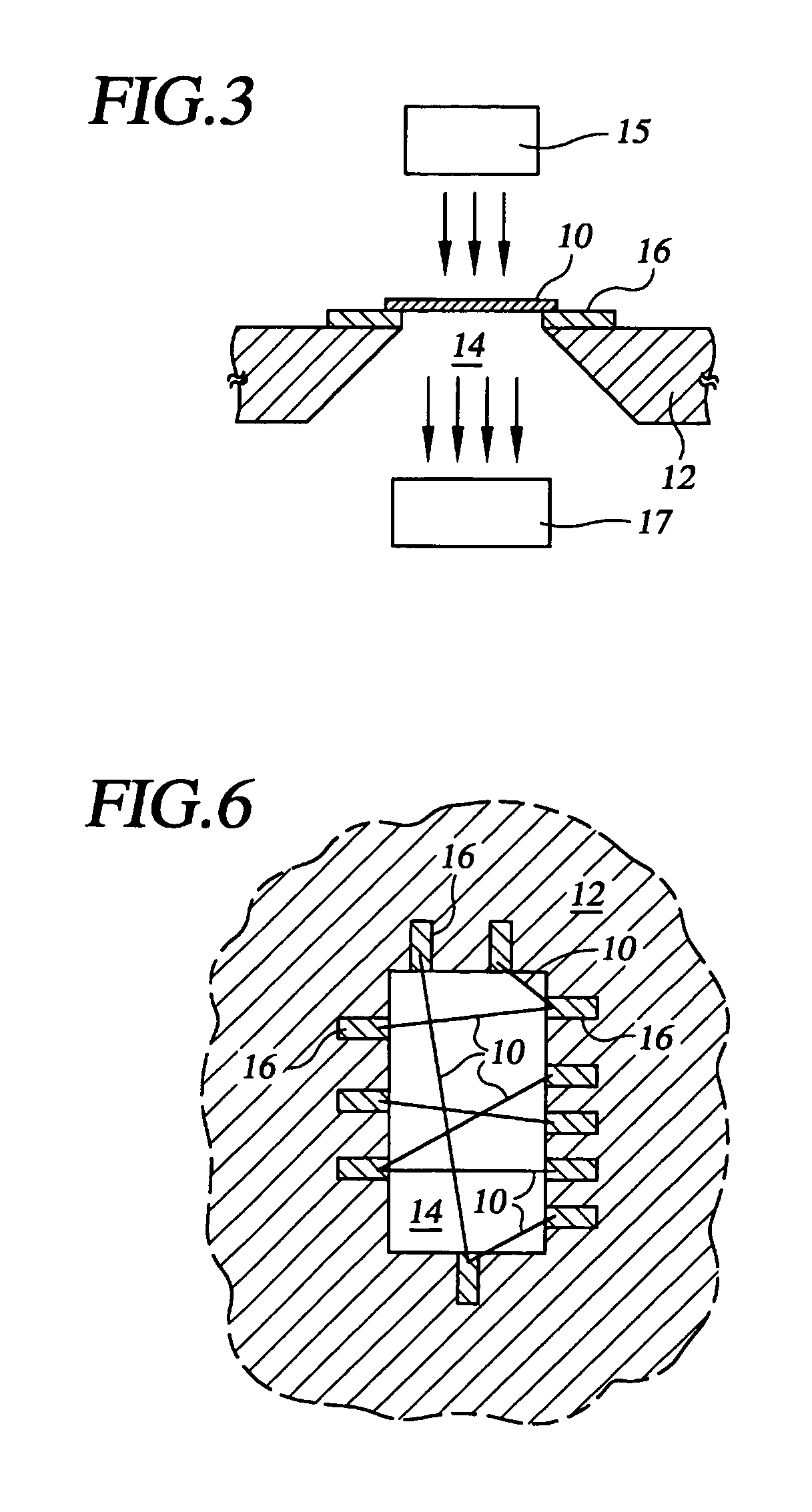
[0061]A silicon nitride membrane having electrically conducting contact pads and a nanotube synthesis catalyst region adjacent to an aperture was fabricated in the manner described above and illustrated in FIGS. 7A-7D. Employing a single lift-off process, two 2 μm-wide contact pads formed of a 50 nm-thick layer of Cr and a 50 nm-thick layer of Pt were formed, with an Fe catalyst layer of 5×10¹⁵ atoms / cm2coverage thermally evaporated atop the contact pad layer. A focused ion beam milling process was employed to mill an aperture through the catalyst layer, the contact pad layers, and the silicon nitride membrane. Nanotube synthesis was then carried out in a 200 sccm flow of methane gas of at a temperature of 900° C. for—less than 5 minutes for various samples.

[0062]With these synthesis conditions, it was found that one or a few single-walled nanotubes were formed suspended across each aperture between electrodes and the overlying catalyst layer, as determined by TEM carried out direct...


PUM

PropertyMeasurementUnit
thicknessaaaaaaaaaa
temperatureaaaaaaaaaa
thicknessaaaaaaaaaa

Abstract

A carbon nanotube device in accordance with the invention includes a support structure including an aperture extending from a front surface to a back surface of the structure. At least one carbon nanotube extends across the aperture and is accessible through the aperture from both the front surface and the back surface of the support structure.

Description

[0001]This application claims the benefit of U.S. Provisional Application No. 60 / 422,041, filed Oct. 29, 2002, the entirety of which is hereby incorporated by reference.STATEMENT REGARDING FEDERALLY SPONSORED RESEARCH[0002]This invention was made with Government support under Contract No. F49620-01-1-0467, awarded by DARPA, and under Contract No. DMR-0073590, awarded by the NSF. The Government has certain rights in the invention.BACKGROUND OF INVENTION[0003]This invention relates generally to the synthesis of carbon nanotubes, and more particularly relates to techniques for controllably fabricating and testing single-walled carbon nanotubes.[0004]Since their discovery, carbon nanotubes have attracted intense research into their electrical and mechanical properties and have been proposed for implementation in a wide range of electronics as well as mechanical and electromechanical applications. In particular it has been demonstrated that carbon nanotubes are distinctly well-suited for...

Claims


Application Information

Patent Timeline
Patent Type & Authority Patents(United States)
IPC IPC(8): H01J1/88C23C16/00H01J1/02B01J23/70B01J35/02B01J37/02C01B3/26C01B31/02H01J1/05H01L27/28
CPCB82Y10/00B82Y30/00B82Y40/00C01B3/26C01B31/0233H01L27/283H01L51/0048H01L51/0508H01L51/0579B01J23/70Y10T428/24331B01J37/0238C01B2202/02C01B2202/06C01B2202/22C01B2203/0277C01B2203/1047C01B2203/1052C01B2203/1241H01J2201/30469B01J35/023C01B32/162H10K19/10H10K85/221H10K10/46H10K10/23
Inventor GOLOVCHENKO, JENE A.PENG, HAIBING
Owner PRESIDENT & FELLOWS OF HARVARD COLLEGE
Why Eureka
Try Eureka