Field emission display and method for fabricating the same

a field emission display and field emission technology, applied in the field of field emission display, can solve the problems of high product cost and long time-consuming for the fabrication of the fed

Inactive Publication Date: 2001-06-28
LG ELECTRONICS INC
View PDF0 Cites 196 Cited by
  • Summary
  • Abstract
  • Description
  • Claims
  • Application Information

AI Technical Summary

Problems solved by technology

And, in fabrication of the FED, because an E-beam is used, screen size can not be any larger than 20", fabrication of the FED takes much time, and product cost is high.

Method used


Image

  • Field emission display and method for fabricating the same
  • Field emission display and method for fabricating the same
  • Field emission display and method for fabricating the same

Examples


embodiment 2

[0036] EMBODIMENT 2

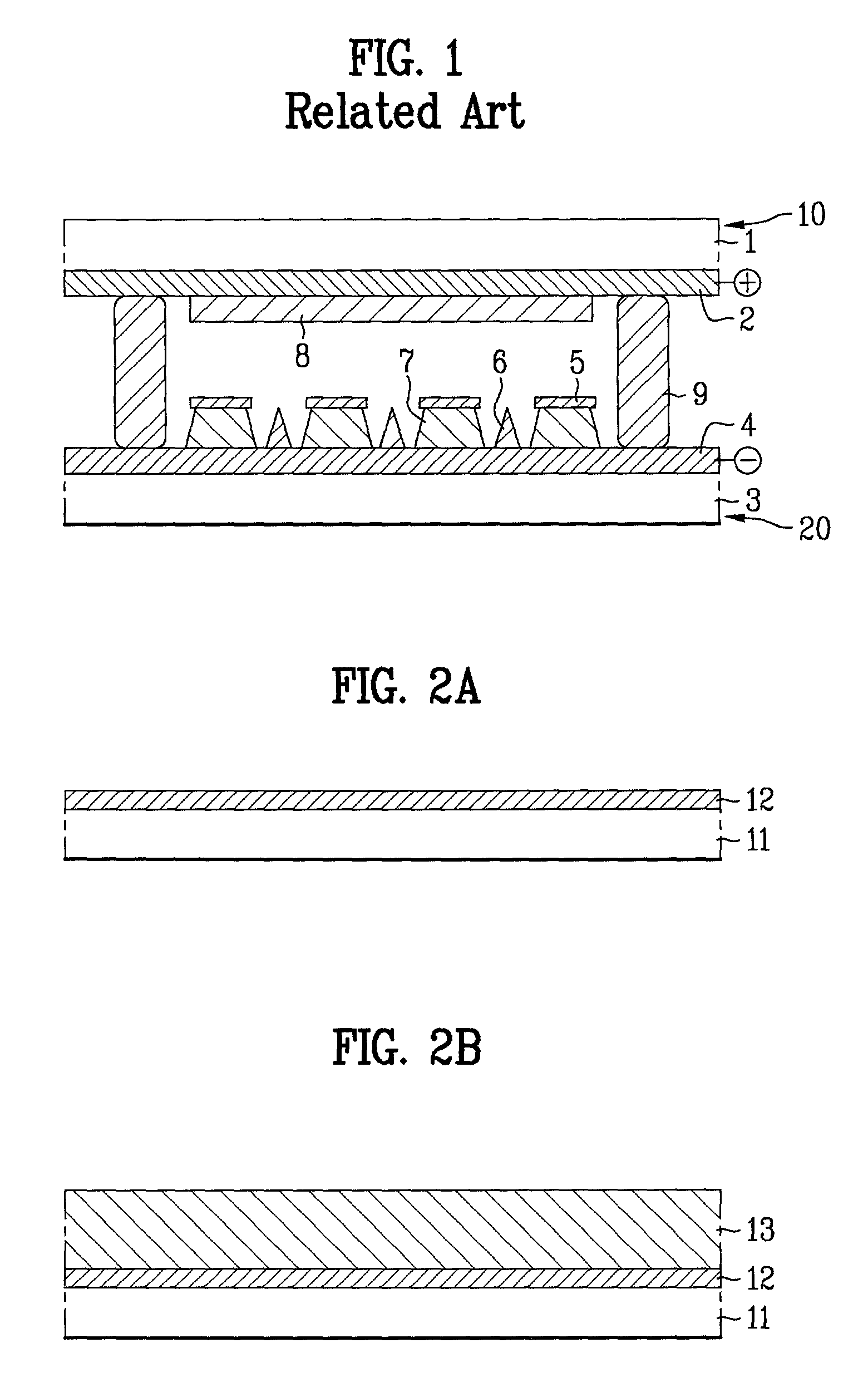
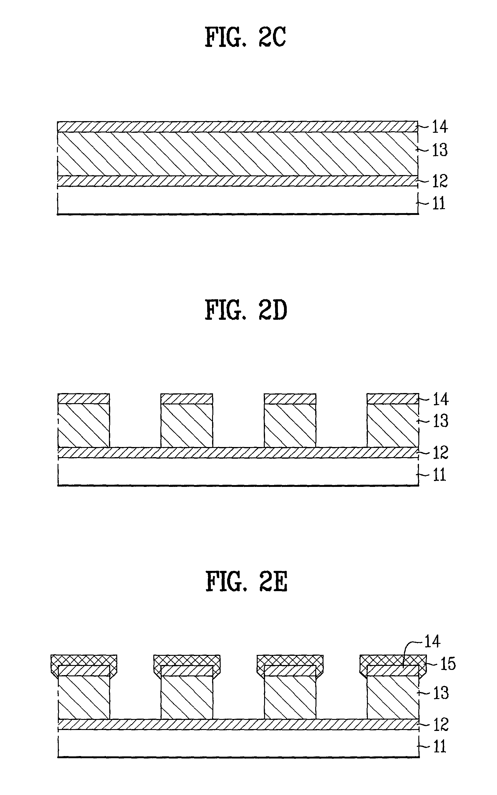
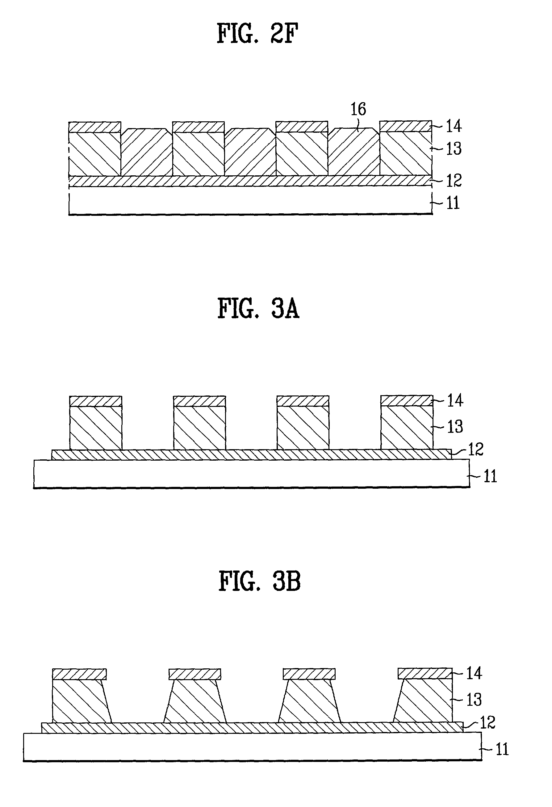
[0037] The second embodiment has process conditions, such as a deposition temperature, vacuum, a time period required for the deposition, the same with the first embodiment, except that the process for forming the emitter region for forming the carbon nanotube as the emitter. That is, different from the first embodiment, in which the sacrificial layer is formed after the gate electrode and the insulating layer are etched, to form the emitter region, the second embodiment shows formation of the emitter region after formation of the sacrificial layer, the gate electrode, and the insulating layer, which will be described in detail. FIGS. 4A.about.4E illustrate sections showing the steps of a process for fabricating a cathode array of a field emission display in accordance with a second preferred embodiment of the present invention.

[0038] Referring to FIG. 4A, an electrode film is formed on a substrate 11 as a cathode electrode 12. As shown in FIG. 4B, a glass paste c...


PUM

PropertyMeasurementUnit
thickaaaaaaaaaa
thicknessaaaaaaaaaa
sizeaaaaaaaaaa

Abstract

Field emission display and method for fabricating the same, the field emission display including a cathode array having a cathode electrode formed on a substrate, insulating layers and carbon nanotube films for use as emitter electrodes formed alternately on the cathode electrode, and a gate electrode formed on the insulating layer, thereby permitting fabrication of a large sized cathode plate at a low cost because the film is formed by screen printing and exposure, which can reduce the cumbersome steps in fabrication of the related art Spindt emitter tip, and both a low voltage and a high voltage FEDs because the carbon nanotube film used as the emitter has a low work function, with an easy and stable electron emission capability.

Description

[0001] 1. Field of the Invention[0002] The present invention relates to a field emission display, and more particularly, to a field emission display which has a stable driving voltage and an excellent productivity, and a method for fabricating the same.[0003] 2. Background of the Related Art[0004] Referring to FIG. 1, a related art Spindt type FED(Field Emission Display) is provided with an anode part 10, a cathode part 20, and a spacer 9 connected between the anode part and the cathode part. The anode part 10 has a face plate 1 which is a glass substrate, an anode 2 which is an ITO (Indium Tin Oxide) thin film electrode formed thereon, and R, G, B stripes 8 of fluorescent materials coated thereon. The cathode part 20 has a base plate 3 of a nonconductive material, an orthogonal matrix of cathode electrode 4 rows and gate electrode 5 columns, FEA(Field Emission Array) emitters 6 matrix addressed between adjacent row electrode and column electrode for emission of electrodes, and an a...

Claims


Application Information

Patent Timeline
Patent Type & Authority Applications(United States)
IPC IPC(8): C03C17/36D01F9/127H01J3/02H01J9/02H01J1/30
CPCB82Y10/00B82Y30/00C03C17/36C03C17/3652C03C17/3671C03C2218/33D01F9/127H01J3/022H01J9/025H01J2201/30469Y10S977/952C01B32/05H01J1/30B82Y40/00
Inventor HAN, SI WOOKKIM, SANG MUN
Owner LG ELECTRONICS INC
Why Eureka
Try Eureka