Pixel unit drive circuit, pixel unit drive method, pixel unit and display device

A driving circuit and pixel unit technology, which is applied in the field of pixel unit and display device, pixel unit driving circuit, can solve the problems of OLED current inconsistency, influence on display effect, uneven luminance of pixel unit, etc., to ensure driving voltage and driving current, The effect of ensuring uniformity and improving quality

Active Publication Date: 2015-03-18
HEFEI BOE OPTOELECTRONICS TECH +1
View PDF10 Cites 0 Cited by
  • Summary
  • Abstract
  • Description
  • Claims
  • Application Information

AI Technical Summary

Problems solved by technology

[0009] From the expression for the current through the OLED (i.e., Equation (1)), it can be seen that this current is not only affected by the data voltage V data controlled by the drive transistor T 2 Threshold voltage V th The impact, that is, the existing 2T1C structure cannot control the threshold voltage V th drift or threshold voltage V th Compensate for inconsistencies
Due to the driving transistor T in each pixel unit driving circuit 2 It is impossible to have completely consistent performance parameters, and there is no adjustment for the drive transistor T in the drive circuit of each pixel unit. 2 The threshold voltage of V th Compensation will inevitably cause inconsistent currents flowing through the OLEDs in each pixel unit, resulting in uneven luminance of each pixel unit, resulting in uneven brightness of the entire display screen and affecting the display effect; moreover, due to the current flowing through the OLEDs in each pixel unit current and data voltage V data It is a nonlinear relationship, so it is not conducive to the adjustment of the gray level of the entire display screen

Method used


Image

  • Pixel unit drive circuit, pixel unit drive method, pixel unit and display device
  • Pixel unit drive circuit, pixel unit drive method, pixel unit and display device
  • Pixel unit drive circuit, pixel unit drive method, pixel unit and display device

Examples


Embodiment 1

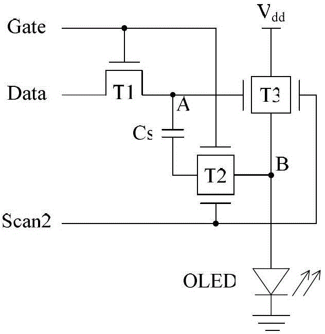
[0056] Such as figure 2 As shown, this embodiment provides a pixel unit driving circuit for driving a light emitting device to emit light, which includes a first thin film transistor T1, a second thin film transistor T2, a third thin film transistor T3 and a storage capacitor Cs.

[0057] Wherein, the first thin film transistor T1 includes a gate, a first pole and a second pole, the gate is connected to the scan line Gate, the first pole is connected to the data line Data, and the second pole is connected to the first Node A is connected.

[0058] The second thin film transistor T2 includes two gates, a first pole and a second pole, that is, the second thin film transistor is a double-gate TFT, one of the two gates is connected to the scanning line Gate, The other gate is connected to the second control line Scan2, the first electrode is connected to the storage capacitor Cs, and the second electrode is connected to the second node B.

[0059] The third thin film transistor...

Embodiment 2

[0093] Such as Figure 5 As shown, this embodiment provides a pixel unit driving circuit for driving OLED to emit light.

[0094] The difference between the pixel unit driving circuit in this embodiment and the pixel unit driving circuit in Embodiment 1 is that: the first node A is connected to the scanning line Gate.

[0095] This embodiment also provides a pixel unit comprising an OLED and the above-mentioned pixel unit driving circuit connected thereto.

[0096] This embodiment also provides a display device comprising a plurality of the above-mentioned pixel units distributed in a matrix.

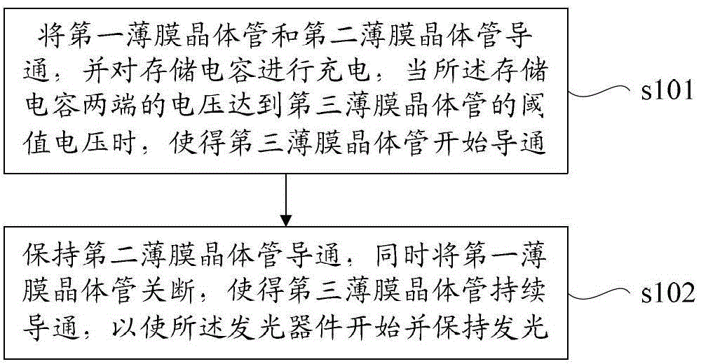
[0097] Such as Figure 6 As shown, this embodiment also provides a pixel unit driving method applied to the above pixel unit driving circuit, including the following steps:

[0098] s201. Turn on the first thin film transistor T1 and the second thin film transistor T2, and pre-charge the first thin film transistor T1, so that the first node A has an initial voltage.

[0099] Specifi...

Embodiment 3

[0128] Such as Figure 8 As shown, this embodiment provides a pixel unit driving circuit for driving OLED to emit light.

[0129] The difference between the pixel unit driving circuit in this embodiment and the pixel unit driving circuit in Embodiment 1 is that: the driving circuit further includes a fourth thin film transistor T4, which includes a gate, a first pole and a second pole; The gate is connected to the first control line Scan1, the first pole is connected to the second node B, and the second pole is grounded.

[0130] This embodiment also provides a pixel unit comprising an OLED and the above-mentioned pixel unit driving circuit connected thereto.

[0131] This embodiment also provides a display device comprising a plurality of the above-mentioned pixel units distributed in a matrix.

[0132] The pixel unit driving circuit described in this embodiment and the matrix formed by the OLEDs connected to it are as follows: Figure 9 As shown, the display device includ...


PUM


Abstract

There are provided a pixel unit driving circuit and driving method, pixel unit and display apparatus. The pixel unit driving circuit is used for driving a light-emitting device to emit light, and comprises a first thin film transistor (T1), a second thin film transistor (T2), a third thin film transistor (T3) and a storage capacitor (Cs). A gate of the first thin film transistor (T1) is connected with a control line (Gate), a first electrode thereof is connected with a data line (Data), and a second electrode thereof is connected with a first node (A). One gate of the second thin film transistor (T2) is connected with the control line (Gate) and the other gate is connected with a second scan line (Scan2), a first electrode thereof is connected with the storage capacitor (Cs), and a second electrode thereof is connected with a second node (B). One gate of the third thin film transistor (T3) is connected with the first node (A) and the other gate is connected with the second scan line (Scan2), a first electrode thereof is connected with a power supply (Vdd), and a second electrode thereof is connected with the second node (B). One terminal of the storage capacitor is connected with the first node (A), and the other terminal is connected with the first electrode of the second thin film transistor (T2). One terminal of the light-emitting device is connected with the second node (B), and the other terminal thereof is grounded. The pixel unit driving circuit can reduce an influence on a driving voltage caused by variations in threshold voltage.

Description

technical field [0001] The present invention relates to the technical field of display driving, in particular to a pixel unit driving circuit, a pixel unit driving method, a pixel unit and a display device. Background technique [0002] OLED (Organic Light-Emitting Diode, organic light-emitting diode) display, also known as organic electroluminescence display, is an emerging flat-panel display device, due to its simple preparation process, low cost, low power consumption, high luminous brightness, Wide range of working temperature, light and thin size, fast response speed, easy to realize color display and large-screen display, easy to realize matching with integrated circuit driver, easy to realize flexible display, etc., so it has broad application prospects. [0003] OLED pixel units in organic electroluminescent displays are generally arranged in a matrix, and can be divided into passive matrix (Passive Matrix-Organic Light Emission Display, PM-OLED for short) driving me...

Claims


Application Information

Patent Timeline
Patent Type & Authority Patents(China)
IPC IPC(8): G09G3/32H05B44/00
CPCG09G2320/045G09G2300/0842G09G2310/0262G09G3/3233G09G2300/0819H05B33/0896H05B45/60
Inventor 孟庆超刘晓燕王文杰苏晓俊
Owner HEFEI BOE OPTOELECTRONICS TECH
Why Eureka
Try Eureka