Gallium nitride semiconductor light emitting element

A technology for light-emitting elements and semiconductors, which is applied in the manufacture of semiconductor devices, semiconductor lasers, and semiconductor/solid-state devices, etc., and can solve the problems of large electric field E, increase of piezoelectric polarization, and increase of driving voltage.

Inactive Publication Date: 2012-04-18
ROHM CO LTD
View PDF1 Cites 0 Cited by
  • Summary
  • Abstract
  • Description
  • Claims
  • Application Information

AI Technical Summary

Problems solved by technology

[0009] But on the p side, as in Figure 10 As shown, since the electric field E is generated from the p-GaN optical guiding layer 44 toward the p-AlGaN cladding layer 45, the holes flowing from the p-AlGaN cladding layer 45 into the p-GaN optical guiding layer 44 are affected by the generated electric field E. Electric repulsion makes it difficult to flow into the MQW active layer 43, resulting in depletion of the carrier and increasing the driving voltage
An increase in driving voltage shortens the lifetime of GaN semiconductor light-emitting devices
[0010] In particular, the p-AlGaN cladding layer 45 contains Mg as a p-type impurity, and when the Mg concentration is 1×10 19 cm -3 Below, the piezoelectric polarization occurring at the interface between the p-GaN optical guiding layer 44 and the p-AlGaN cladding layer 45 sharply increases, Figure 10 The electric field E shown can become unusually large and thus become a problem

Method used


Image

  • Gallium nitride semiconductor light emitting element
  • Gallium nitride semiconductor light emitting element
  • Gallium nitride semiconductor light emitting element

Examples


Embodiment Construction

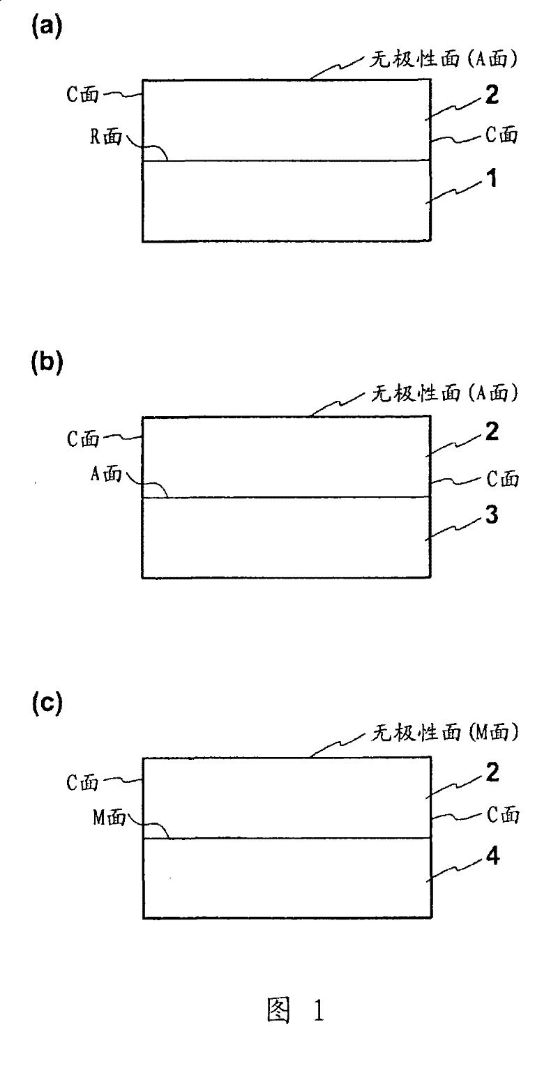
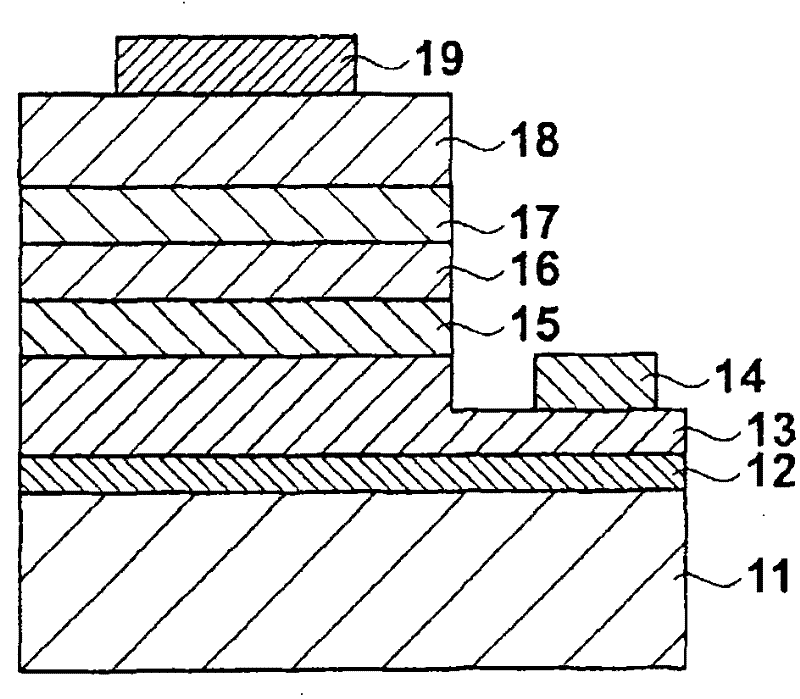
[0031] Hereinafter, an embodiment of the present invention will be described with reference to the drawings. figure 1 The schematic structure of the gallium nitride semiconductor light emitting device of the present invention is shown. figure 1 The gallium nitride semiconductor light-emitting element of (a) is a gallium nitride semiconductor crystal 2 including a light-emitting region formed on a sapphire substrate 1. The gallium nitride semiconductor crystal 2 is formed on the R surface (1-102) of the sapphire substrate 1 by the MOCVD method or the like, and its growth surface is grown on the A surface. Reference Figure 8 , 9 It can be seen that the A plane is not a Ga polar plane and an N (nitrogen) polar plane, but a non-polar plane.

[0032] In addition, Japanese Patent Laid-Open No. 2000-216497 shown in Patent Document 1 describes that a GaN-based semiconductor layer is laminated on the A side and M side of a sapphire substrate, and the growth surface can be made M side o...


PUM


Abstract

Provided is a gallium nitride semiconductor light emitting element wherein a drive voltage is stabilized by reducing spontaneous polarization generated on an interface between an AlGaN semiconductor layer and a GaN semiconductor layer and carrier depletion due to piezo polarization. On a plane (R) of a sapphire substrate (1), a gallium nitride semiconductor crystal (2) including a light emitting region is formed. In other constitution, on a plane (A) or a plane (M) of GaN substrates (3, 4), the gallium nitride semiconductor crystal (2) is formed. Since the growing planes of these gallium nitride semiconductor crystals (2) are nonpolar planes and not an N (nitrogen) polar plane nor a Ga polar plane, an electric field caused by spontaneous polarization and piezo polarization generated on a GaN / AlGaN interface on a p-side can be reduced and carrier depletion can be eliminated.

Description

Technical field [0001] The present invention relates to a gallium nitride semiconductor light emitting element using GaN. Background technique [0002] As semiconductor light emitting elements such as semiconductor laser elements and light emitting diodes that emit blue or violet light, there are gallium nitride semiconductor light emitting elements. When manufacturing GaN-based semiconductor elements, it is difficult to manufacture a substrate made of GaN, so a GaN-based semiconductor layer is epitaxially grown on a substrate made of sapphire, SiC, Si, or the like. [0003] For example, using MOCVD (metal organic vapor growth method), an undoped GaN buffer layer, n-GaN contact layer, n-AlGaN cladding layer, n-GaN optical guide layer, and n-GaN optical guide layer are sequentially formed on the (0001) surface of a sapphire substrate. InGaN multiple quantum well (MQW) active layer, etc., p-GaN optical guide layer, p-AlGaN cladding layer, p-GaN contact layer, etc. are sequentially f...

Claims


Application Information

Patent Timeline
Patent Type & Authority Patents(China)
IPC IPC(8): H01S5/343H01L33/00H01L33/06H01L33/16H01L33/20H01L33/32
CPCH01L33/16H01S5/22H01L33/007H01S5/34333H01L21/02433H01L21/02609H01S5/3216H01L21/0242H01S5/3202B82Y20/00H01L21/0254H01S5/32025
Inventor 中原健
Owner ROHM CO LTD
Why Eureka
Try Eureka