Methods of providing a family of related integrated circuits of different sizes

Active Publication Date: 2009-03-03
XILINX INC
View PDF43 Cites 11 Cited by
  • Summary
  • Abstract
  • Description
  • Claims
  • Application Information

AI Technical Summary

Benefits of technology

[0010]The invention provides methods of manufacturing a family of packaged integrated circuits (ICs) having at least two different logic capacities, and multi-product dies that can be used to implement such methods. A first IC die includes at least two different portions, of which at least one portion can be deliberately rendered non-operational in some manner (e.g., non-functional, inaccessible, and/or non-programmable) within the package. A first set of the first IC dies are packaged such that both portions of the dies are operational. A second set of the first IC dies are packaged such that only the first port

Problems solved by technology

Therefore, purchasing mask sets for

Method used


Image

  • Methods of providing a family of related integrated circuits of different sizes
  • Methods of providing a family of related integrated circuits of different sizes
  • Methods of providing a family of related integrated circuits of different sizes

Examples


Example

DETAILED DESCRIPTION OF THE DRAWINGS

[0047]The present invention is applicable to a variety of integrated circuits (ICs).

[0048]The present invention has been found to be particularly applicable and beneficial for programmable logic devices (PLDs). An appreciation of the present invention is presented by way of specific examples utilizing PLDs such as field programmable gate arrays (FPGAs). However, many aspects of the present invention are not so limited.

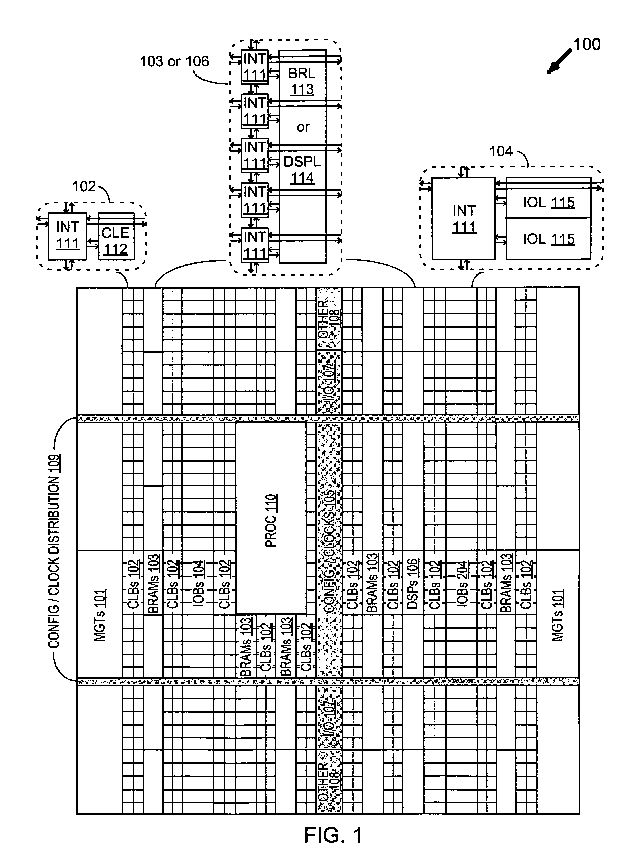
[0049]As noted above, advanced FPGAs can include several different types of programmable logic blocks in the array. For example, FIG. 1 illustrates an FPGA architecture 100 that includes a large number of different programmable tiles including multi-gigabit transceivers (MGTs 101), configurable logic blocks (CLBs 102), random access memory blocks (BRAMs 103), input / output blocks (IOBs 104), configuration and clocking logic (CONFIG / CLOCKS 105), digital signal processing blocks (DSPs 106), specialized input / output blocks (I / O 107) (e.g...


PUM


Abstract

Methods of manufacturing a family of packaged integrated circuits (ICs) having at least two different logic capacities. A first IC die includes two different portions, of which at least one portion can be deliberately rendered non-operational in some manner (e.g., non-functional, inaccessible, and/or non-programmable) within the package. A first set of the first IC dies are packaged such that both portions of the dies are operational. A second set of the first IC dies are packaged such that only the first portion of each die is operational. Once the first and second sets are packaged and the second set of ICs has been evaluated, a decision is made whether or not to manufacture a second IC die that includes the first portion of the first die, while excluding the second portion.

Description

FIELD OF THE INVENTION[0001]The invention relates to integrated circuit devices (ICs). More particularly, the invention relates to structures and methods of providing multiple ICs of different sizes (e.g., a family of related programmable logic devices) from a single die.BACKGROUND OF THE INVENTION[0002]Programmable logic devices (PLDs) are a well-known type of integrated circuit that can be programmed to perform specified logic functions. One type of PLD, the field programmable gate array (FPGA), typically includes an array of programmable tiles. These programmable tiles can include, for example, input / output blocks (IOBs), configurable logic blocks (CLBs), dedicated random access memory blocks (BRAM), multipliers, digital signal processing blocks (DSPs), processors, clock managers, delay lock loops (DLLs), and so forth.[0003]Each programmable tile typically includes both programmable interconnect and programmable logic. The programmable interconnect typically includes a large numb...

Claims


Application Information

Patent Timeline
IPC IPC(8): H01L21/44
CPCH01L23/00H01L2924/0002H01L2924/00
Inventor GOETTING, F. ERICHBAUER, TREVOR J.MCGUIRE, PATRICK J.TALLEY, BRUCE E.WU, PAUL YING-FUNGYOUNG, STEVEN P.
Owner XILINX INC
Why Eureka
Try Eureka