Cascode circuit employing a depletion-mode, GaN-based FET

a gan-based, depletion-mode technology, applied in the direction of transistors, pulse techniques, electronic switching, etc., can solve the problems of -based enhanced-mode fets, generally not satisfactory, and excessive consumption of power, and achieve the effect of increasing band gap

Active Publication Date: 2009-03-10
POWER INTEGRATIONS INC
View PDF2 Cites 55 Cited by
  • Summary
  • Abstract
  • Description
  • Claims
  • Application Information

AI Technical Summary

Problems solved by technology

Such an arrangement can consume an excessive amount of power.
Unfortunately, while attempts have been made to manufacture GaN-based enhanced-mode FETs, they have generally not been satisfactory because of problems such as poor on-state conductances and poor breakdown voltages.

Method used


Image

  • Cascode circuit employing a depletion-mode, GaN-based FET
  • Cascode circuit employing a depletion-mode, GaN-based FET
  • Cascode circuit employing a depletion-mode, GaN-based FET

Examples


Embodiment Construction

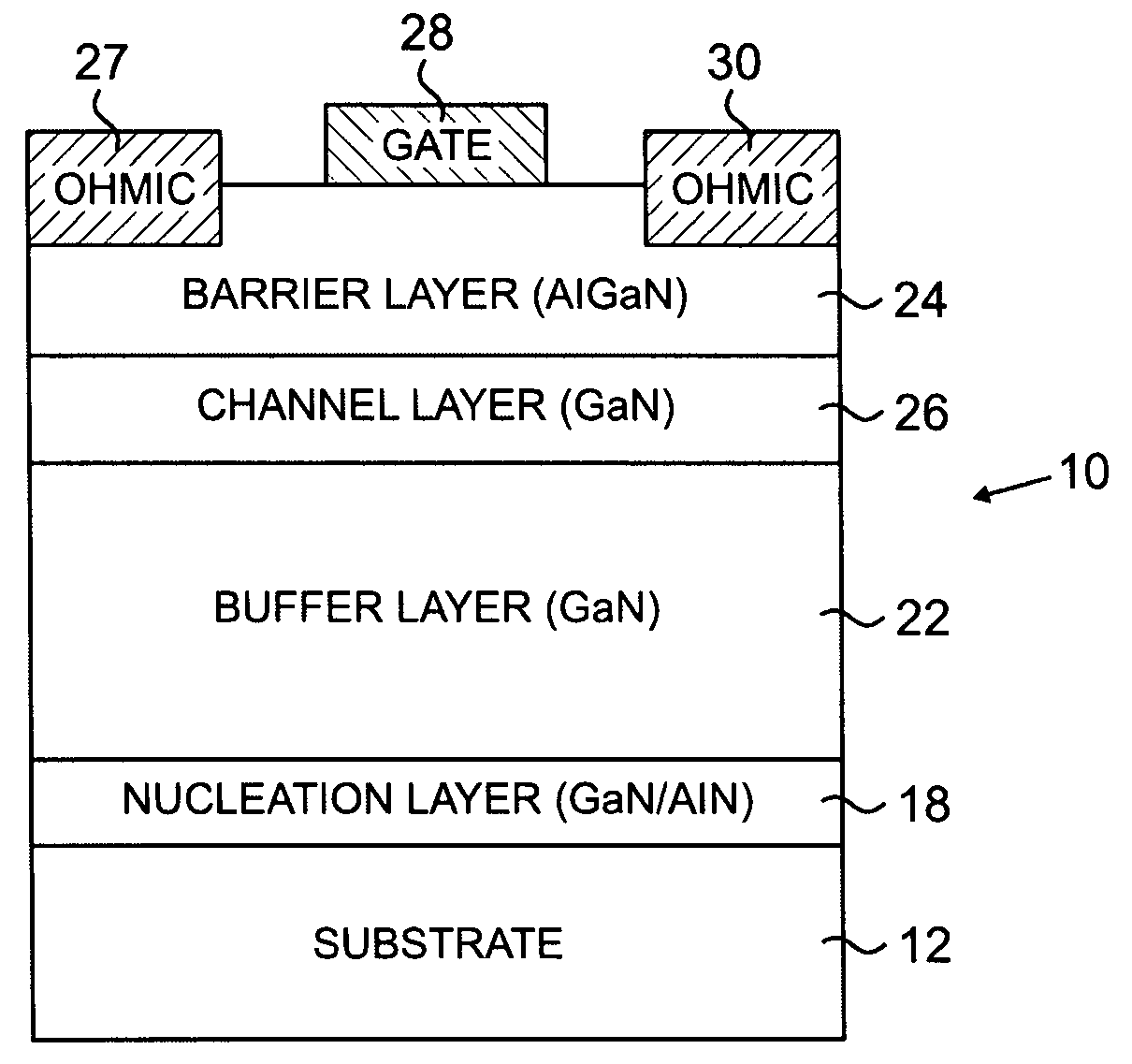
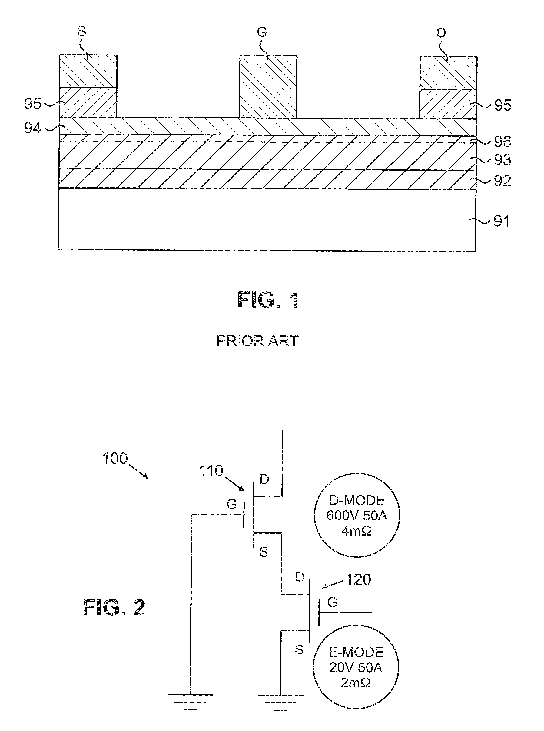
[0026]The present inventor has recognized that instead of fabricating a semiconductor GaN-based, enhanced-mode FET semiconductor structure, the desired operating characteristics of such a structure can be readily achieved using a GaN-based, depletion mode structure having similar operating characteristics. That is, as detailed below, the present invention combines a GaN-based, depletion-mode FET with one or more other components so that the resulting device acts as an enhancement-mode FET. For instance, in one particular embodiment of the invention the GaN-based depletion mode FET is arranged in series with an enhancement mode FET to provide an enhancement mode device that in other respects has the characteristics of the GaN-based, depletion mode FET.

[0027]Individual FET devices can be connected in various known ways, e.g., common source, common gate, common drain, source follower, etc. to provide different characteristics of operation as desired to suit a particular purpose. Two su...


PUM


Abstract

A circuit includes an input drain, source and gate nodes. The circuit also includes a group III nitride depletion mode FET having a source, drain and gate, wherein the gate of the depletion mode FET is coupled to a potential that maintains the depletion mode FET in its on-state. In addition, the circuit further includes an enhancement mode FET having a source, drain and gate. The source of the depletion mode FET is serially coupled to the drain of the enhancement mode FET. The drain of the depletion mode FET serves as the input drain node, the source of the enhancement mode FET serves as the input source node and the gate of the enhancement mode FET serves as the input gate node.

Description

RELATED APPLICATIONS[0001]This application is related to U.S. patent application Ser. No. 11 / 725,823, entitled “Termination and Contact Structures For A High Voltage GaN-Based Heterojunction Transistor,” filed on even date herewith and incorporated by reference in its entirety herein.[0002]This application is also related to U.S. patent application Ser. No. 11 / 725,820, entitled “High-Voltage GaN-Based Heterojunction Transistor Structure and Method of Forming Same,” filed on even date herewith and incorporated by reference in its entirety herein.FIELD OF THE INVENTION [0003]The present invention relates generally to a Group III nitride compound semiconductor FET such as a GaN-based FET, and more particularly to a circuit that employs a depletion mode GaN-based FET and which functions as an enhancement mode FET.BACKGROUND OF THE INVENTION [0004]GaN-based FETs using a wide bandgap semiconductor such as GaN, AlGaN, InGaN, AlGaN, AlInGaN and the like have received much attention as a pow...

Claims


Application Information

Patent Timeline
Patent Type & Authority Patents(United States)
IPC IPC(8): H01L31/0328
CPCH01L27/0605H01L29/2003H01L29/66462H03K19/0952H03F1/226H03K17/567H03K19/09482H01L29/7786H01L27/0883H01L2924/1033
Inventor MURPHY, MICHAEL
Owner POWER INTEGRATIONS INC
Why Eureka
Try Eureka