
CASCODE STRUCTURES WITH GaN CAP LAYERS

a cascode structure and gan cap technology, applied in the direction of transistors, semiconductor devices, electrical apparatus, etc., can solve the problems of limiting the performance of these devices, the the resulting difference between dc and rf characteristics,

Active Publication Date: 2014-12-11
CREE INC
View PDF13 Cites 52 Cited by
  • Summary
  • Abstract
  • Description
  • Claims
  • Application Information

AI Technical Summary

Benefits of technology

The present invention provides a new way to create transistors using a dual-gate structure. In this structure, the second stage gate does not need to be separately biased. The transistor includes a plurality of active semiconductor layers on a substrate, with a first gate between the source and drain, and a second gate between the first gate and the drain. A cap layer separates the second gate from the semiconductor layers. This structure allows for improved performance and reliability of the transistor. The invention also includes an integrated circuit that includes a transistor with a plurality of active semiconductor layers on a substrate, with a first gate and a second gate between the first gate and the drain, and a cap layer between the second gate and the semiconductor layers. The technical effects of this innovation include improved performance and reliability of transistors and more efficient integrated circuits.

Problems solved by technology

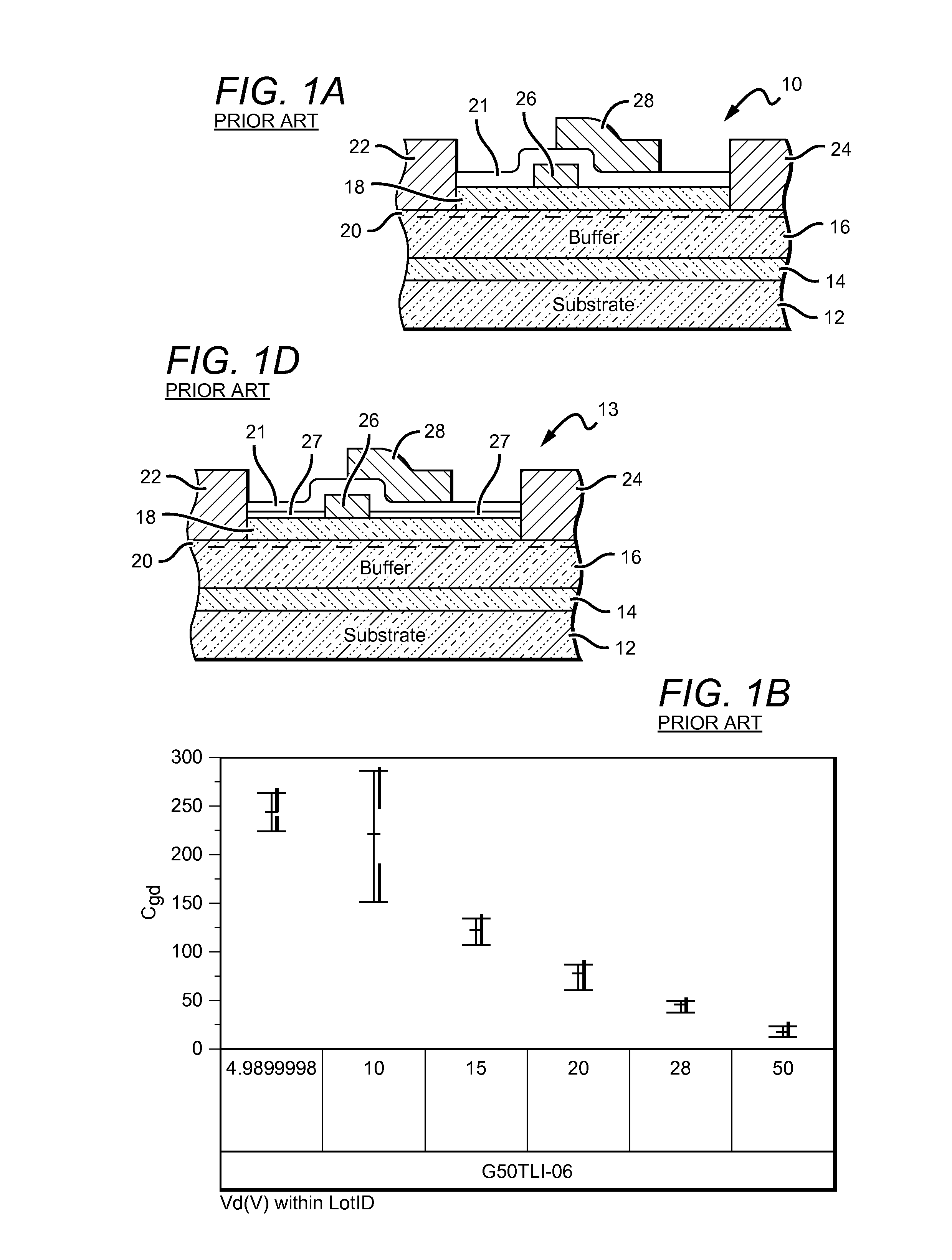
However, these more familiar semiconductor materials may not be well-suited for high power and / or high frequency applications, for example, due to their relatively small bandgaps (1.12 eV for Si and 1.42 for GaAs at room temperature) and relatively small breakdown voltages.
Electron trapping and the resulting difference between DC and RF characteristics can be a limiting factor in the performance of these devices.
However, due to the high electric fields existing in these structures, charge trapping can still be a concern.
This can result in a reduction of the electric field on the gate-to-drain side of the transistor, thereby increasing breakdown voltage and reducing the high-field trapping effect.
However, transistors with gate-to-drain field plates can exhibit relatively poor reliability performance, particularly at class C (or higher class) operation where the electric field on the source side of the gate becomes significant.
If the second gate in such an arrangement is grounded, then the current flow can be limited.
However, separately biasing the second stage leads to added complexity and cost.
Electron mobility within the 2DEG 20 can therefore be negatively affected by physical impurities at this interface, such as roughness.
The increase in separation can result in increased electron mobility and reduced trapping, but typically will result in a lowered sheet charge density.

Method used


Image

  • CASCODE STRUCTURES WITH GaN CAP LAYERS
  • CASCODE STRUCTURES WITH GaN CAP LAYERS
  • CASCODE STRUCTURES WITH GaN CAP LAYERS

Examples


Embodiment Construction

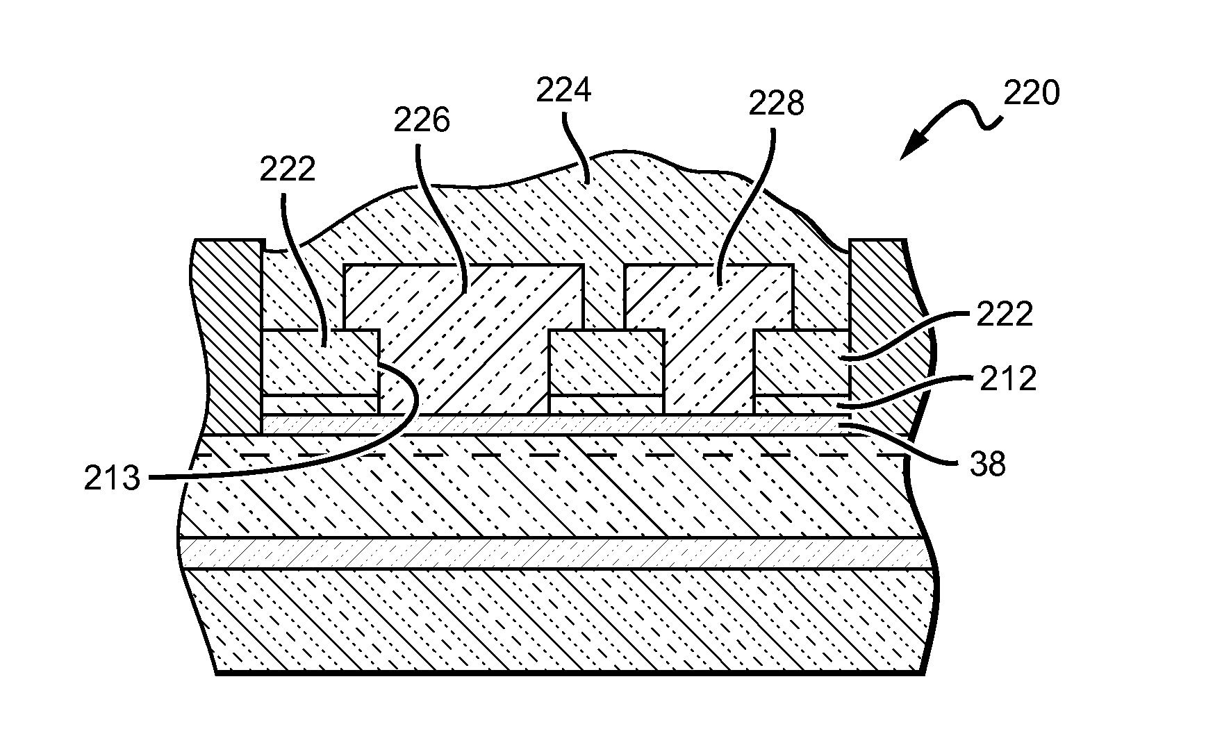
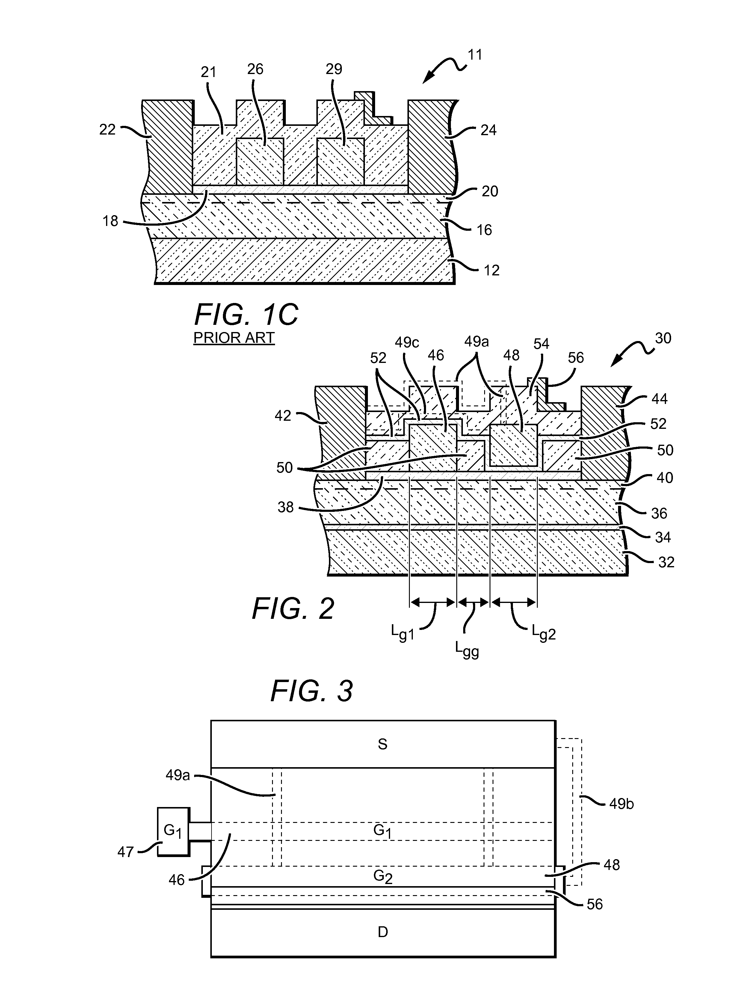
[0049]The present invention provides structures, such as a dual-gate transistor or HEMT cascade structure, that provide lower feedback capacitance and improved linearity at reduced complexity and cost. These structures, such as a GaN-based dual-gate HEMT, can provide high voltage, high current, and high gain operation with improved linearity. The present invention is generally directed to cascode structures wherein a second stage gate is separated from the barrier layer by a relatively thin spacer layer, causing the second stage to have a more negative threshold voltage than the first stage. In one embodiment, the second stage includes a cavity in a spacer layer which exposes the active region; a thin spacer layer is deposited over the active region, and the second stage gate fills the remainder of the cavity. The second stage gate can then be grounded, such as through a connection to the source, and the need for separately biasing the second stage gate is eliminated.

[0050]The prese...


PUM


Abstract

A transistor device including a cap layer is described. One embodiment of such a device includes cap layer between a gate and a semiconductor layer. In one embodiment, the thickness of the cap layer is between 5 nm and 100 nm. In another embodiment, the cap layer can be doped, such as delta-doped or doped in a region remote from the semiconductor layer. Devices according to the present invention can show capacitances which are less drain bias dependent, resulting in improved linearity.

Description

[0001]This application is a continuation-in-part of and claims the benefit of U.S. patent application Ser. No. 13 / 913,490, filed on Jun. 9, 2013 and entitled “Cascode Structures for GaN HEMTs,” and is a continuation-in-part of and claims the benefit of U.S. patent application Ser. No. 13 / 929,487, filed on Jun. 27, 2013 and entitled “Recessed Field Plate Transistor Structures.” Each of the above applications is fully incorporated by reference herein in its entirety.BACKGROUND OF THE INVENTION[0002]1. Field of the Invention[0003]The present invention relates to cascode structures and particularly to dual-gate transistors having an insulating layer below one gate. The present invention also relates to transistors including a field plate and particularly to transistors having a field plate relatively near the semiconductor layers. The present invention also relates to cascade structures and particularly to dual-gate transistors having a cap layer below one gate.[0004]2. Description of t...

Claims


Application Information

Patent Timeline
Patent Type & Authority Applications(United States)
IPC IPC(8): H01L29/778H01L27/088
CPCH01L27/088H01L29/778H01L29/402H01L29/42316H01L29/7787H01L29/2003
Inventor SRIRAM, SAPTHARISHI
Owner CREE INC
Learn More