Check patentability & draft patents in minutes with Patsnap Eureka AI!

Incremental solver for modeling an integrated circuit

a technology of incremental solver and integrated circuit, which is applied in the field of integrative circuits, can solve the problems of difficult for ic designers to assess the effect of a relatively small incremental change in a design, the complexity of the problem of rf integrated circuit extraction, and the inability to accurately solve the problem of incremental change, etc., and achieve the effect of flexible solution and accurate solution

Active Publication Date: 2009-03-17
CADENCE DESIGN SYST INC
View PDF2 Cites 3 Cited by
  • Summary
  • Abstract
  • Description
  • Claims
  • Application Information

AI Technical Summary

Benefits of technology

Enables accurate and efficient IC modeling for incremental design changes, reducing computational time and improving the usability of modeling tools for design purposes by reusing calculated values and maintaining designations of nearby and far-away mesh-element pairs.

Problems solved by technology

In general, these parasitic effects are undesired component interactions that result from increasingly compact and complex circuit designs, and their modeling (or extraction) has become increasingly important for verifying designs.
However, RF integrated circuits have been particularly problematic for extraction methodologies due to the use of embedded passive elements.
However, these fullwave solutions are generally computationally intensive and take a significant amount of time because of the large size of the corresponding matrices.
Furthermore, it is generally difficult for IC designers to assess the effect of a relatively small incremental change in a design without a substantially redoing the calculations for the fullwave solution.

Method used


Image

  • Incremental solver for modeling an integrated circuit
  • Incremental solver for modeling an integrated circuit
  • Incremental solver for modeling an integrated circuit

Examples


Embodiment Construction

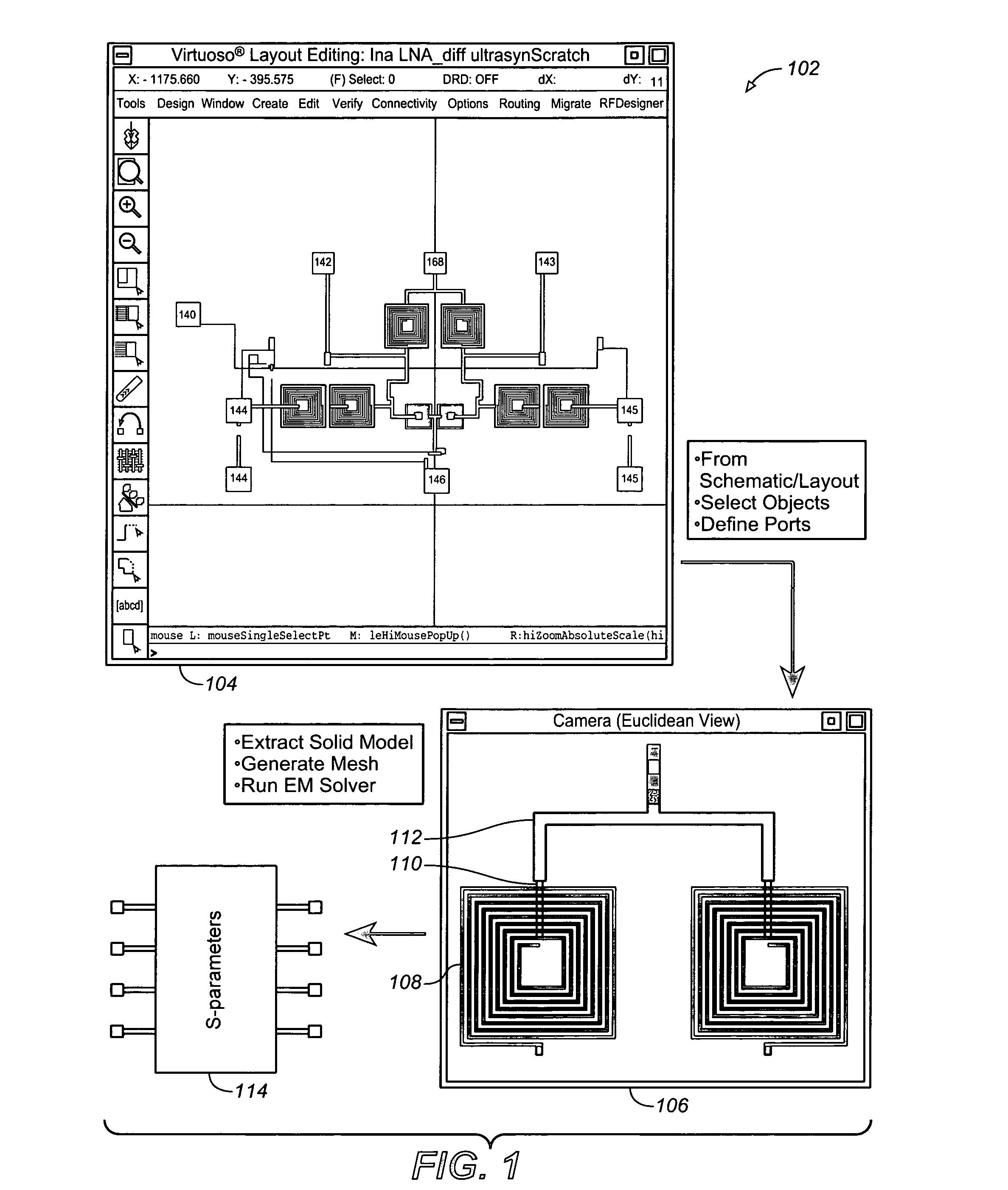
[0044]FIG. 1 shows an operational overview 102 for an embodiment of the present invention. From an IC (integrated circuit) schematic or layout 104, an extraction 106 is selected for modeling. Typically this extraction, which may also be considered as a layout, includes a number of objects 108 (e.g., inductors as shown) with associated ports 110 and interconnect 112. As discussed below in further detail, the modeling process for the extraction 106 includes determining a solid model, generating a corresponding mesh (e.g., a discretization) and running an EM (electromagnetic) solver to estimate parasitic effects by determining corresponding S-parameters 114 (or some alternative characterization).

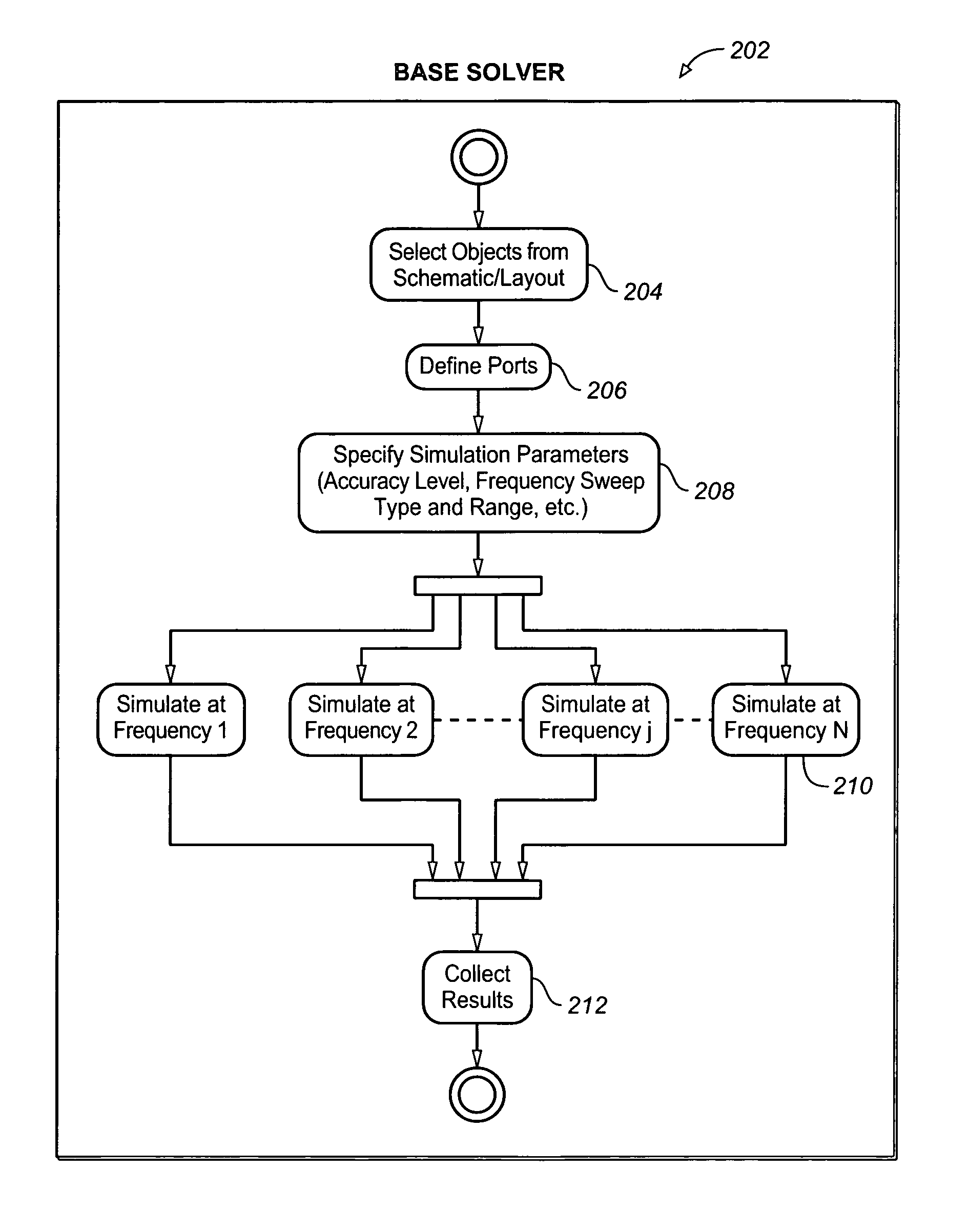
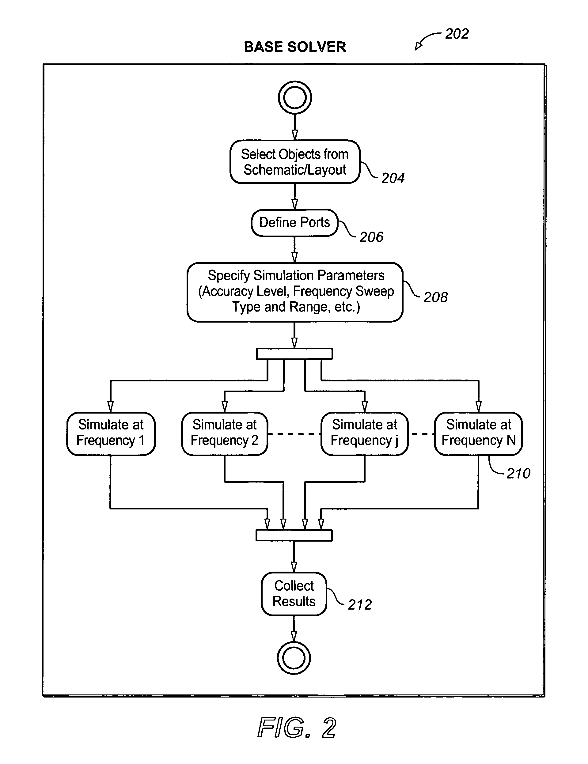
[0045]FIG. 2 shows an exemplary flow diagram 202 for a base solver (e.g., a basic IC modeler for relating voltages and currents). First objects are selected 204 from a schematic or layout. Next ports are defined 206. Next simulation parameters are specified 208 (e.g., accuracy level, frequency ...


PUM


Abstract

A system and method for modeling an IC (integrated circuit) employs a mesh model and a grid model for separating impedance effects between nearby and far-away pairs of mesh elements. Models for relating currents and voltages can be incrementally adapted from other designs or design elements in applications including mixed-signal, analog and RF (radio frequency) circuits.

Description

BACKGROUND OF THE INVENTION[0001]1. Field of Invention[0002]The present invention relates to integrated circuits and more particularly to modeling current and voltage relationships in integrated circuits.[0003]2. Description of Related Art[0004]Parasitic extraction has been an important part of integrated circuit (IC) design verification for at least a decade, and the sophistication of the extraction process has increased over this time. In general, these parasitic effects are undesired component interactions that result from increasingly compact and complex circuit designs, and their modeling (or extraction) has become increasingly important for verifying designs.[0005]The assumption that devices themselves did not interact with one another and could be modeled by their compact models remained valid until relatively recently. However, the interaction between devices via the substrate has turned out to be critical to the performance of especially mixed-signal, analog and RF (radio f...

Claims


Application Information

Patent Timeline
Patent Type & Authority Patents(United States)
IPC IPC(8): G06F17/50
CPCG06F17/5036G06F30/367
Inventor DENGI, ENIS AYKUTLING, FENGSONG, BENHARRIS, WARREN
Owner CADENCE DESIGN SYST INC
Features
  • R&D
  • Intellectual Property
  • Life Sciences
  • Materials
  • Tech Scout
  • Unparalleled Data Quality
  • Higher Quality Content
  • 60% Fewer Hallucinations
Learn More