Flexible substrates for organic devices

a flexible substrate and organic technology, applied in the direction of sustainable manufacturing/processing, identification means, instruments, etc., can solve the problems of insufficient barrier for long-life organic devices, the oxygen and water permeability of even the most impermeable transparent plastic substrates (thin films) presently available is too high to be sufficient as a barrier, and the deposited thin ito (or other conductive oxide coating) is prone to cracking

Inactive Publication Date: 2009-04-07
CAMBRIDGE DISPLAY TECH LTD
View PDF3 Cites 10 Cited by
  • Summary
  • Abstract
  • Description
  • Claims
  • Application Information

AI Technical Summary

Benefits of technology

[0008]It is an aim of the present invention to provide an improved substrate for an electronic or optoelectronic device including at least one electrically active organic layer, which avoids or at least reduces the problems of the prior art.
[0009]According to one aspect of the present invention there is provided a transparent or substantially transparent formable and / or flexible component for use as an outer protective element in such an organic device, which component is a composite structure comprising a layer of glass of a thickness ≦200 μm and a layer of plastic. In this connection the formability of the component allows it to deviate from full planarity by bending and / or twisting so it can adapt to the shape or form of some other object. Its flexibility allows it to be bent without detrimentally affecting its barrier properties.
[0040]It is often the case that the problems with handling thin glass arise from picking up glass sheets at the edges where a crack can start very easily. In order to avoid this, one embodiment of the present invention provides that the plastic layer extends beyond the edges of the glass layer in the composite so that the plastic part only can be used to pick up the composite structure. This reduces cracking possibilities and keeps the glass layer untouched.
[0045]Additional functionality can be incorporated into the plastic layer. For example, the plastic layer can comprise a plastic polariser sheet, a contrast-enhancing filter-laminate, have anti-reflective properties, colour filter properties or colour conversion properties. For example, it would be possible to have a device in which the light emitting layer emits blue light and in which the laminate contains, for example, red or green fluorescent molecules which absorb the blue and re-emit in the red or green. Alternatively or additionally, the plastic layer can be designed to block undesired ambient light and / or have scattering particles so that wave guiding is reduced and the brightness of the device is increased. Where possible, such additional functionalities could be incorporated in the glass layer. Where a third plastic layer is provided in the composite structure, this allows the possibility of two different types of plastic layers, providing the possibility for incorporating different additional functionalities into the different layers.
[0046]The present application thus describes transparent substrates and encapsulation films for use in organic devices which avoids or at least reduces the problems of prior art and provides substrates and films which have both good transparency and good barrier properties and which can also be handled without great risk of deteriorating the continuity of the substrate and its barrier properties.

Problems solved by technology

However, for OLEDs fabricated on transparent plastic foils it is extremely difficult to encapsulate the transparent side against the ingress of ambient reactive species.
The oxygen and water permeabilities of even the most impermeable transparent plastic substrates (thin films) presently available are too high to be sufficient as a barrier for long life OLED devices.
However, these thin ITO (or other conductive oxide coatings) deposited onto thin flexible plastic substrates are prone to “cracking” if the substrates are not handled with the greatest care.
In addition to that, such cracks in the ITO coating may also result in an undesired deterioration of the surface flatness of the coating.
This requirement to avoid cracking of the ITO coating puts severe constraints on the handling of the substrates and devices and hence the manufacturing process.
However, such thin glass, although of a composition and specially manufactured to reduce brittleness, is still extremely difficult to handle and can very easily break if not handled with the greatest care.
This puts severe limitations on the use of thin flexible glass as substrates for OLEDs due to the difficulty of manufacturing.

Method used


Image

  • Flexible substrates for organic devices
  • Flexible substrates for organic devices
  • Flexible substrates for organic devices

Examples


Embodiment Construction

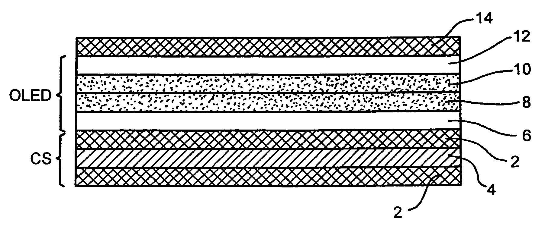
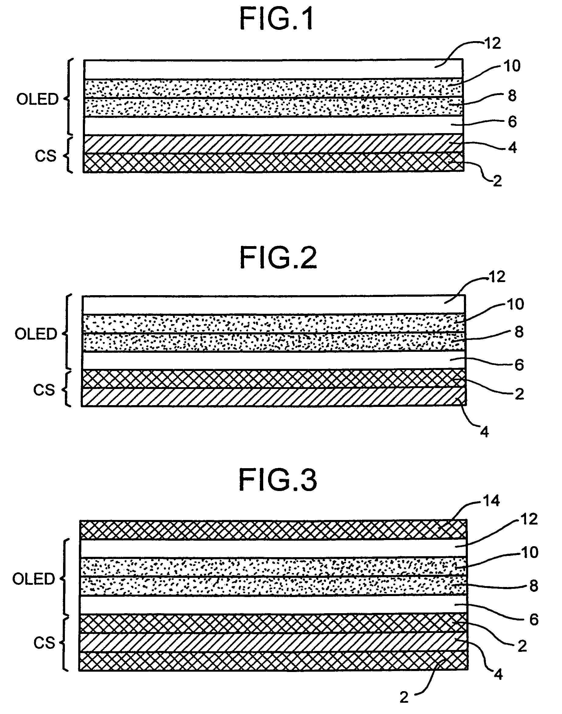
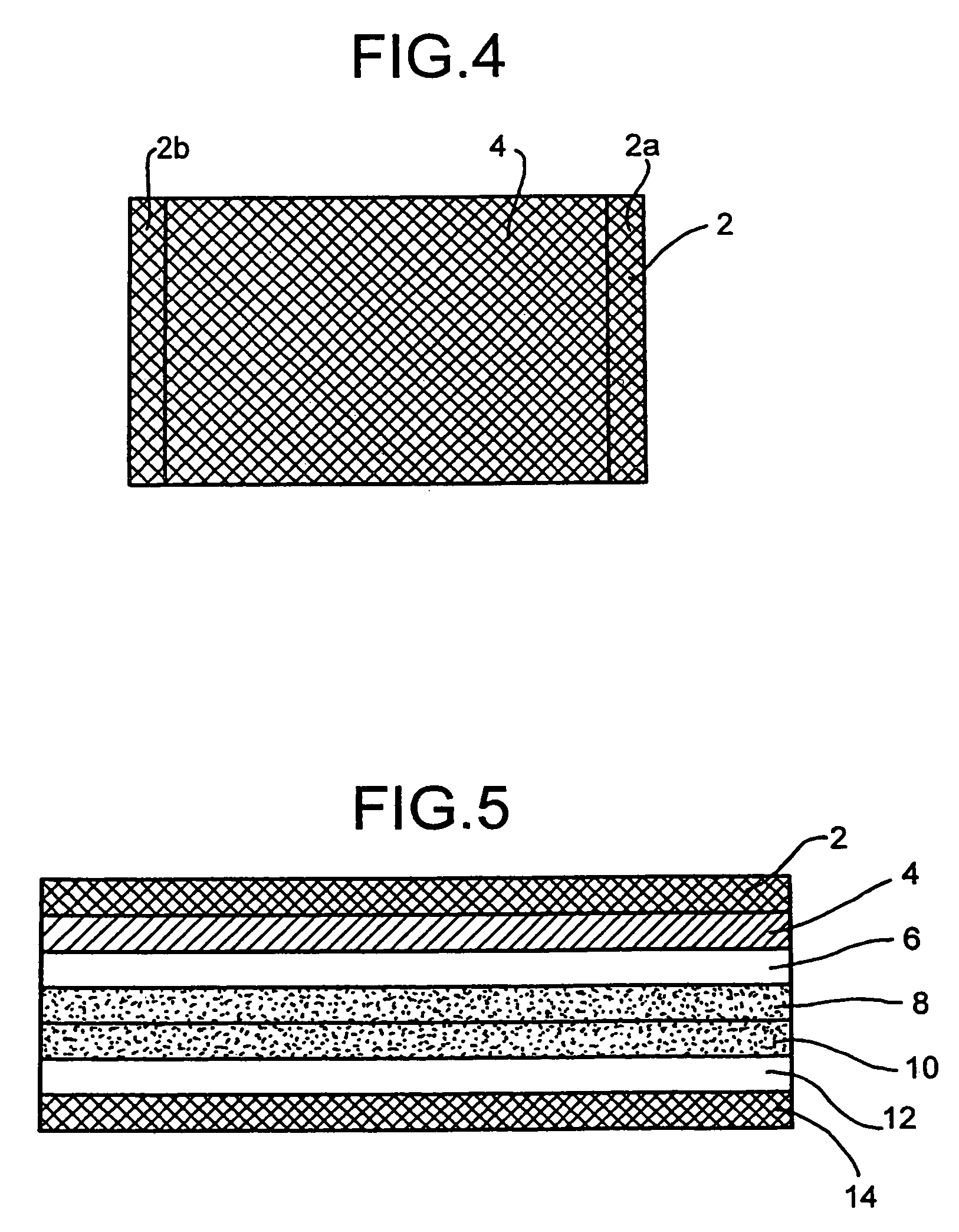
[0053]FIG. 1 illustrates an organic light-emitting device with a composite structure as its substrate. In FIG. 1, OLED is used to denote the organic light-emitting device and CS is used to denote the composite structure. The composite structure comprises a plastic layer 2 and a glass layer 4. The organic light-emitting device OLED comprises a first electrode layer 6, in this case an anode formed of indium tin oxide, a first thin film of an organic light emissive material 8 (in this case PPV), a second thin film of an organic material 10 (e.g. MEHPPV, and a second electrode layer 12 in this case a cathode, for example of a calcium layer capped by an aluminium layer. The second layer of organic material can be a light-emissive layer or a charge transport layer or have some other purpose. Further organic light-emissive layers can be provided.

[0054]As an alternative to the arrangement described above, layer 8 could be a charge transport layer such as polyethylenedioxythiophene doped wit...


PUM

PropertyMeasurementUnit
thicknessaaaaaaaaaa
thickaaaaaaaaaa
thickaaaaaaaaaa

Abstract

A transparent or substantially transparent formable and / or flexible component for use as an outer protective element in an electronic or opto electronic device including at least one electrically active organic layer, which component is a composite structure comprising a layer of glass of a thickness less than or equal to 200 microns and a layer of plastic.

Description

RELATED APPLICATIONS[0001]This is a continuation of U.S. Ser. No. 10 / 326,977, filed Dec. 24, 2002, pending; which is a continuation of U.S. Ser. No. 09 / 283,424, filed Apr. 1, 1999 (now U.S. Pat. 6,592,969); which claims priority from GB9807149.1, filed Apr. 2, 1998; all of which are incorporated herein by reference.FIELD OF THE INVENTION[0002]This invention relates to flexible substrates for organic devices and particularly but not exclusively to organic light emitting devices (OLEDs) and to OLEDs fabricated on flexible substrates.[0003]Organic light-emitting devices such as described in U.S. Pat. No. 5,247,190 or in U.S. Pat. No. 4,539,507, the contents of which are incorporated herein by reference, have great potential for use in various display applications. According to one method, an OLED is fabricated by coating a glass or plastic substrate with a transparent first electrode (anode) such as indium tin oxide (ITO). At least one layer of a thin film of an electroluminescent orga...

Claims


Application Information

Patent Timeline
Patent Type & Authority Patents(United States)
IPC IPC(8): H05B33/02B32B7/02G09F9/30B32B17/10H01L51/50H01L51/52H05B33/10H05B33/12H05B33/14
CPCH01L51/5012H01L51/5237B32B17/10018B32B17/10027B32B17/10174B32B17/10211B32B17/10541H01L51/0097Y10T428/24975H01L51/52H01L2251/5338Y10S428/917Y02E10/549Y10T428/26Y10T428/24802H01L51/5036Y02P70/50H10K77/111H10K50/125H10K50/80H10K50/11H10K50/8423H10K50/841H10K50/844H10K2102/311B32B2457/206B32B2307/412
Inventor BURROUGHES, JEREMY HENLEYDEVINE, PETER
Owner CAMBRIDGE DISPLAY TECH LTD
Why Eureka
Try Eureka