Wafer structure for electronic integrated circuit manufacturing

a technology of electronic integrated circuits and wafers, applied in the direction of basic electric elements, electrical apparatus, semiconductor devices, etc., can solve the problems of ineffective neutron bombardment of existing ics, and achieve the reduction of minority carrier lifetime in the base region, the effect of improving the hardening of fully completed integrated circuits, and increasing the total ionizing dos

Active Publication Date: 2013-02-28
CAES COLORADO SPRINGS LLC
View PDF3 Cites 7 Cited by
  • Summary
  • Abstract
  • Description
  • Claims
  • Application Information

AI Technical Summary

Benefits of technology

[0013]According to embodiments of the present invention, hardening of such existing IC's against both total ionizing dose (TID) radiation effects (including, neutrons and the secondary particles generated by the neutrons) and single event effects (SEE) is made possible by both pinning the surface potential of the potentially affected regions in the integrated circuit, and by limiting the generation of electron hole pairs produced in sensitive regions of the integrated circuit due to bombardment of the IC with heavy ions, gamma rays, x-rays, electrons, protons, or other types of ionizing radiation as is described herein.
[0014]Further, the embodiments of the present invention can be combined in such a way as to provide both an improved substrate to manufacture existing circuits, or to provide hardening of newly designed circuits either alone or in combination with existing designs. Embodiments of the present invention also provide improved hardening of fully completed integrated circuits via high energy monoenergetic neutron bombardment. Monoenergetic neutron bombardment allows for creation of the defects to reduce the minority carrier lifetime in the base regions of the parasitic SCR structures inherent in modern CMOS IC's. Previous work on neutron bombardment of existing ICs proved largely ineffective due to the concomitant large amount of total ionizing radiation delivered along with the neutron irradiation. A new family of neutron generators based on a deuterium-tritium (D-T) or deuterium-deuterium (D-D) reaction are capable of delivering orders of magnitude more neutron irradiation without a significant increase in total ionizing dose.

Problems solved by technology

Previous work on neutron bombardment of existing ICs proved largely ineffective due to the concomitant large amount of total ionizing radiation delivered along with the neutron irradiation.

Method used


Image

  • Wafer structure for electronic integrated circuit manufacturing
  • Wafer structure for electronic integrated circuit manufacturing
  • Wafer structure for electronic integrated circuit manufacturing

Examples


first embodiment

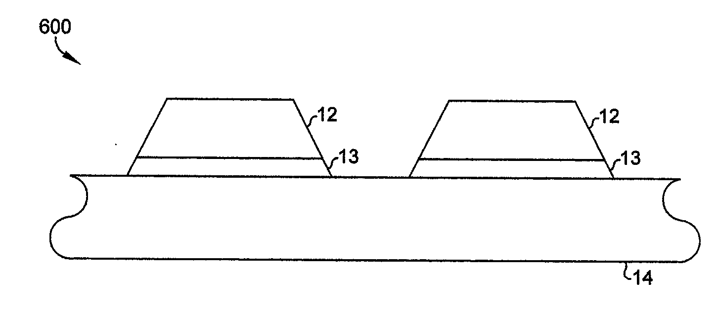
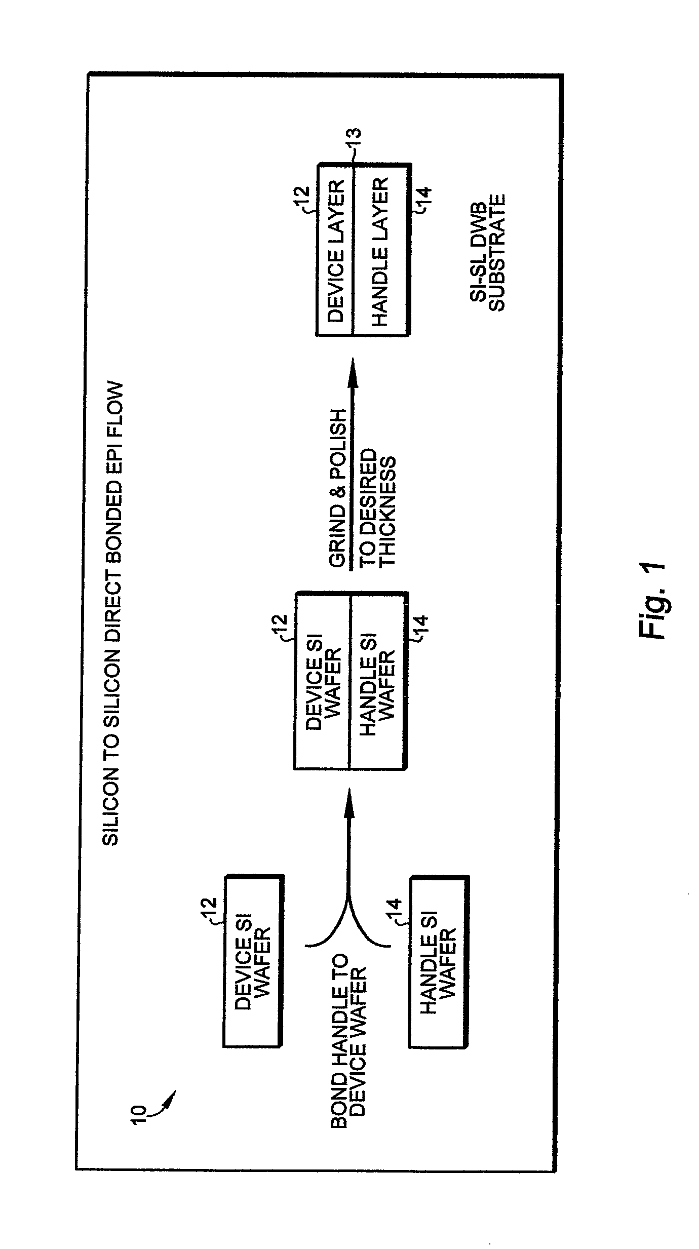
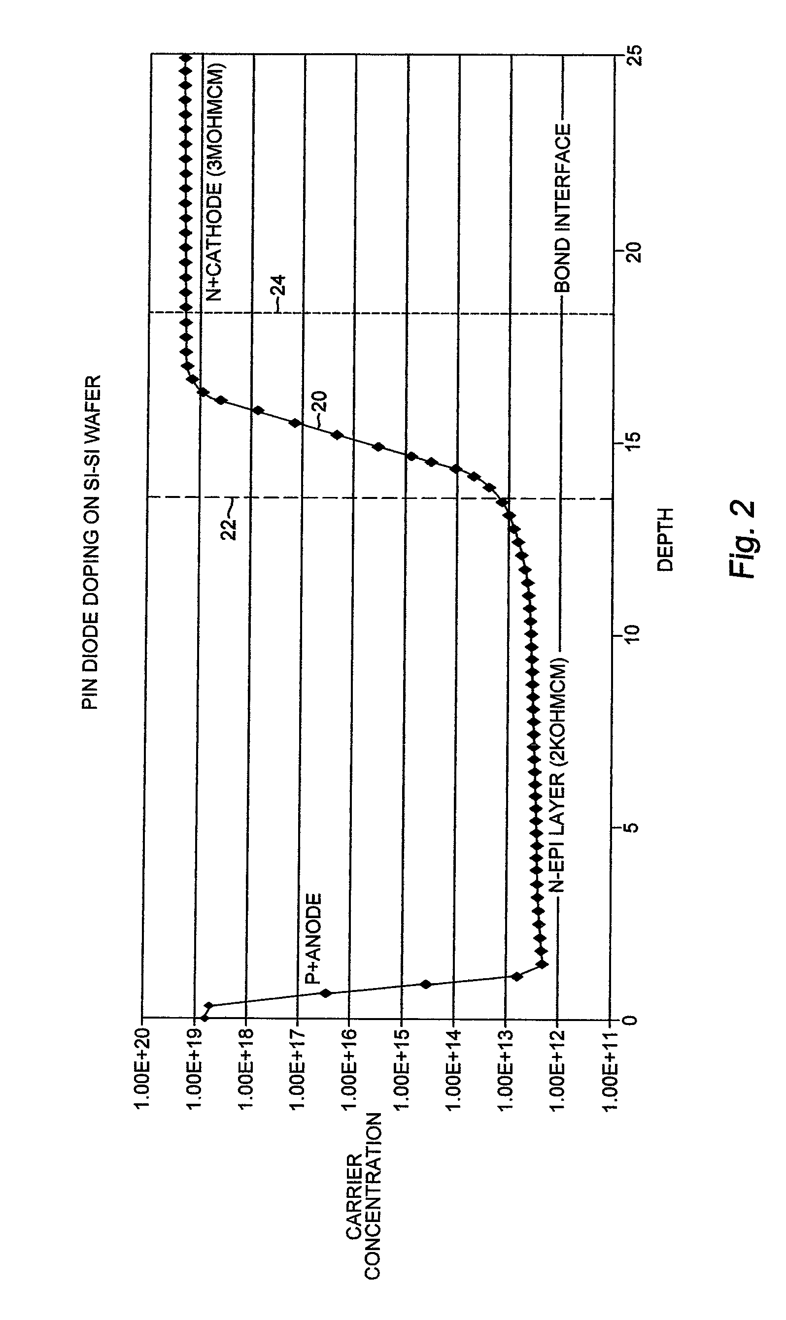
[0028]In the present invention, a wafer structure includes a first region (from the device wafer) 12 having at least one major surface, a thickness and a conductivity profile of a first conductivity type substantially perpendicular to the at least one major surface, a second region (from the handle wafer) 14 having a thickness and a second conductivity profile of the first conductivity type of the first region 12, such second conductivity profile being substantially different than the conductivity profile of the first region 12, such that the second region 14 is in electrical contact with the first region opposite the major surface of the first region, an interface region 13 being formed between the first region 12 and the second region 13, and impurity sites placed in at least one of the first region 12, the second region 14, and the interface region 13, such impurity sites being substantially electrically inactive over a predetermined temperature range (−75° C. to +200° C. degrees...

second embodiment

[0040]According to the invention, a wafer structure includes a first region 12 having at least one major surface, a thickness, and a conductivity profile of a first conductivity type substantially perpendicular to said at least one major surface, a second region 14 having a thickness, and a second conductivity profile of a second conductivity type opposite to that of said first region, such that said second region is in electrical contact with said first region opposite the major surface of said first region, an interface region 13 formed between said first region and said second region, and impurity sites placed in at least one of said first region, said second region, and said interface region, such impurity sites being substantially electrically inactive over a temperature range, wherein the conductivity profile of said first region transitions abruptly to the conductivity profile of said second region within the interface region. The primary difference between this embodiment an...

sixth embodiment

[0044]In the invention, forming of the impurity sites by high energy bombardment is emphasized. The following description will generally refer again to FIG. 1, and also to additional FIGS. 7 and 8.

[0045]Thus, in FIG. 1, a wafer structure 10 includes a first region 12 having at least one major surface, a thickness, and a conductivity profile of a first conductivity type substantially perpendicular to said at least one major surface, a second region 14 having a thickness, and a second conductivity profile of the first conductivity type of said first region, such second conductivity profile being substantially different than the conductivity profile of said first region, such that said second region is in electrical contact with said first region opposite the major surface of said first region, an interface region 13 formed between said first region and said second region, and impurity sites placed in at least one of said first region, said second region, and said interface region, by ...


PUM


Abstract

A bonded wafer structure having a handle wafer, a device wafer, and an interface region with an abrupt transition between the conductivity profile of the device wafer and the handle wafer is used for making semiconductor devices. The improved doping profile of the bonded wafer structure is well suited for use in the manufacture of integrated circuits. The bonded wafer structure is especially suited for making radiation-hardened integrated circuits.

Description

RELATED CASE INFORMATION[0001]This application is related to:[0002]application Ser. No. xx / xxx,xxx, (Attorney Docket No. UTMC158.1);[0003]application Ser. No. xx / xxx,xxx, (Attorney Docket No. UTMC158.3);[0004]application Ser. No. xx / xxx,xxx, (Attorney Docket No. UTMC158.4);[0005]application Ser. No. xx / xxx,xxx, (Attorney Docket No. UTMC158.5); and[0006]application Ser. No. xx / xxx,xxx, (Attorney Docket No. UTMC159),[0007]all of which are entitled “WAFER STRUCTURE FOR ELECTRONIC INTEGRATED CIRCUIT MANUFACTURING”, all of which are herein incorporated by reference as if set forth in their entireties, and all of which are filed concurrently.FIELD OF THE INVENTION[0008]The present invention relates to wafer structures used for the manufacture of electronic integrated circuits, and more particularly to semiconductor integrated circuits, including complementary metal-oxide-silicon (CMOS) integrated circuits.BACKGROUND OF THE INVENTION[0009]It is well known that ionizing radiation (such as g...

Claims


Application Information

Patent Timeline
Patent Type & Authority Applications(United States)
IPC IPC(8): H01L29/06H01L21/30H01L21/322
CPCH01L29/66136H01L29/868H01L21/187H01L21/263H01L29/78H01L27/0921H01L21/304
Inventor KERWIN, DAVID B.BENEDETTO, JOSEPH
Owner CAES COLORADO SPRINGS LLC
Why Eureka
Try Eureka