

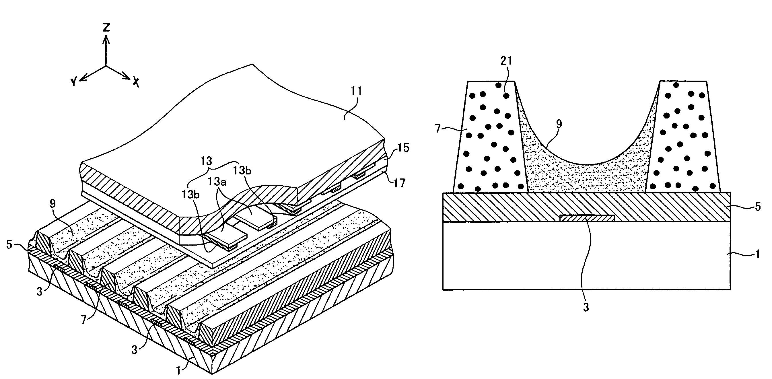
Plasma display panel
a technology of display panel and plasma, which is applied in the field of plasma display panel, can solve the problems of deteriorating brightness and efficiency of phosphors, affecting reliability including the lifespan of phosphors, and deteriorating phosphor layers of residual carbon and water in discharge cells
- Summary
- Abstract
- Description
- Claims
- Application Information
AI Technical Summary
Problems solved by technology
Method used
Image

Examples
example 1
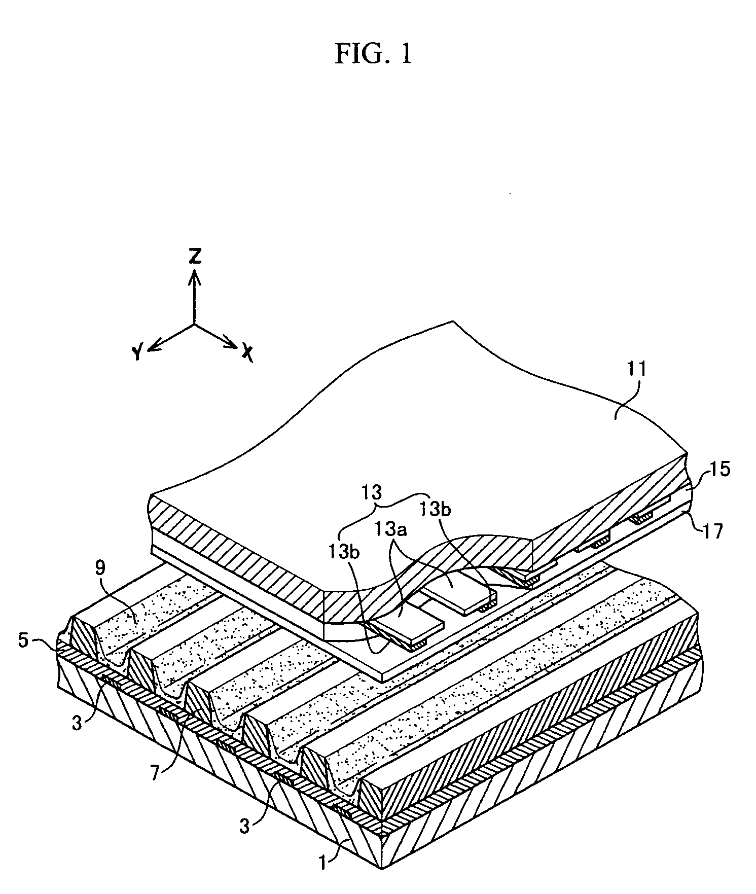
[0039]40 wt % of a glass frit (manufactured by Daejoo Electron Materials Co., Ltd., DGC562S), 50 wt % of ethyl cellulose, 8 wt % of butylcarbitolacetate, and 2 wt % of lithium ion exchange mordenite (manufactured by Aekyung Chemical Co., Ltd., Valfor 100) were mixed to provide a composition for making a barrier rib.
[0040]The composition for making the barrier rib was coated on a dielectric layer, which is formed on the first substrate and address electrodes, to a thickness of 300 μm, and was fired at 550° C. for 30 minutes to provide a barrier rib layer. A photosensitive film (BF704, TOKYO OHKA CHEMICALS) was laminated on the battier rib layer, and then was exposed and developed to make a predetermined pattern of the photosensitive film on the first substrate. The barrier rib layer is exposed through a portion on which the photosensitive film is removed.
[0041]The first substrate having the pattern of the photosensitive film was introduced into an etching device equipped with a spray...
example 2
[0044]A plasma display panel formed with a barrier rib was fabricated by the same method as described in Example 1, except that 2 wt % of a sodium ion exchange mordenite (manufactured by Aekyung Chemical Co., Ltd., Valfor 100) was used instead of the lithium ion exchange mordenite in the composition for making a barrier rib.
example 3
[0045]A plasma display panel formed with a barrier rib was fabricated by the same method as described in Example 1, except that 2 wt % of a calcium ion exchange faujasite (manufactured by Aekyung Chemical Co., Ltd., Folfor 100) was used instead of the lithium ion exchange mordenite in the composition for making a barrier rib.
PUM
 Abstract
Description
Claims
Application Information