Integrated circuit with through-die via interface for die stacking

a technology of throughdie via and stacking die, which is applied in the field of integrated circuits with throughdie via interfaces for die stacking, can solve the problems of incompatibility with fpga designed for flip-chip packaging, difficult if not impossible to mount a second ic to the face side of the fpga die,

Active Publication Date: 2009-04-14
XILINX INC
View PDF9 Cites 58 Cited by
  • Summary
  • Abstract
  • Description
  • Claims
  • Application Information

AI Technical Summary

Problems solved by technology

This approach, however, is incompatible with FPGAs designed for flip-chip packaging.
Such bump contacts make it difficult if not impossible to mount a second IC to the face side of the FPGA die.

Method used


Image

  • Integrated circuit with through-die via interface for die stacking
  • Integrated circuit with through-die via interface for die stacking
  • Integrated circuit with through-die via interface for die stacking

Examples


Embodiment Construction

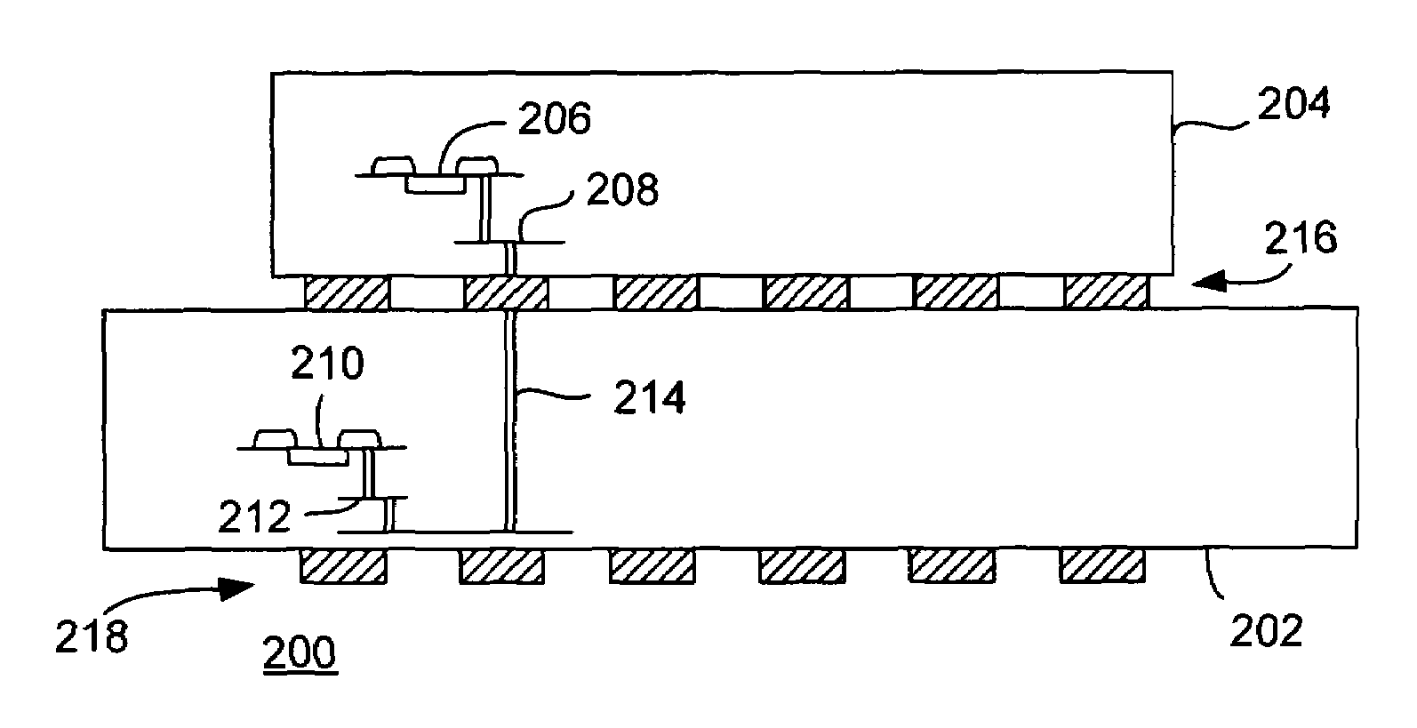
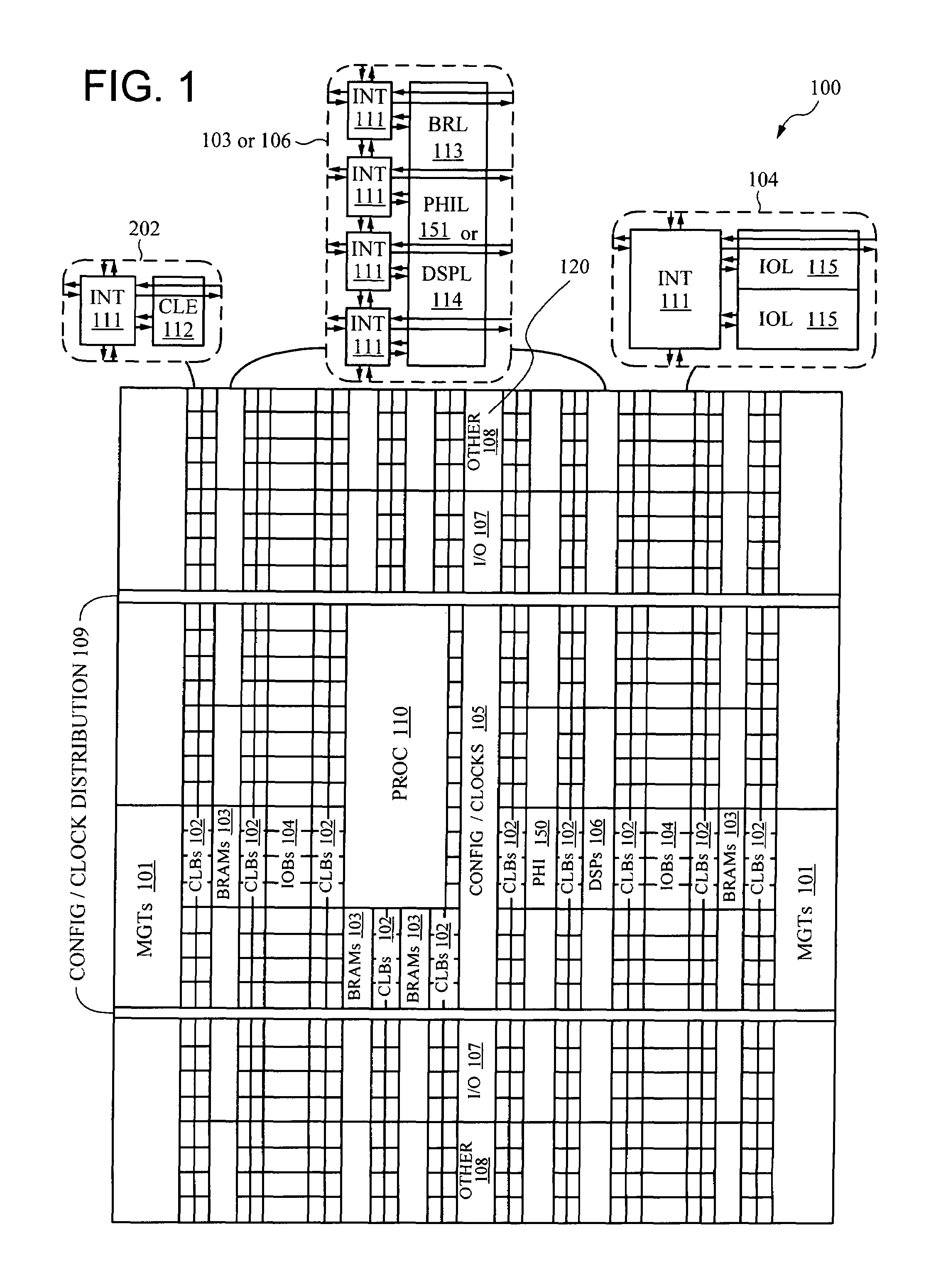
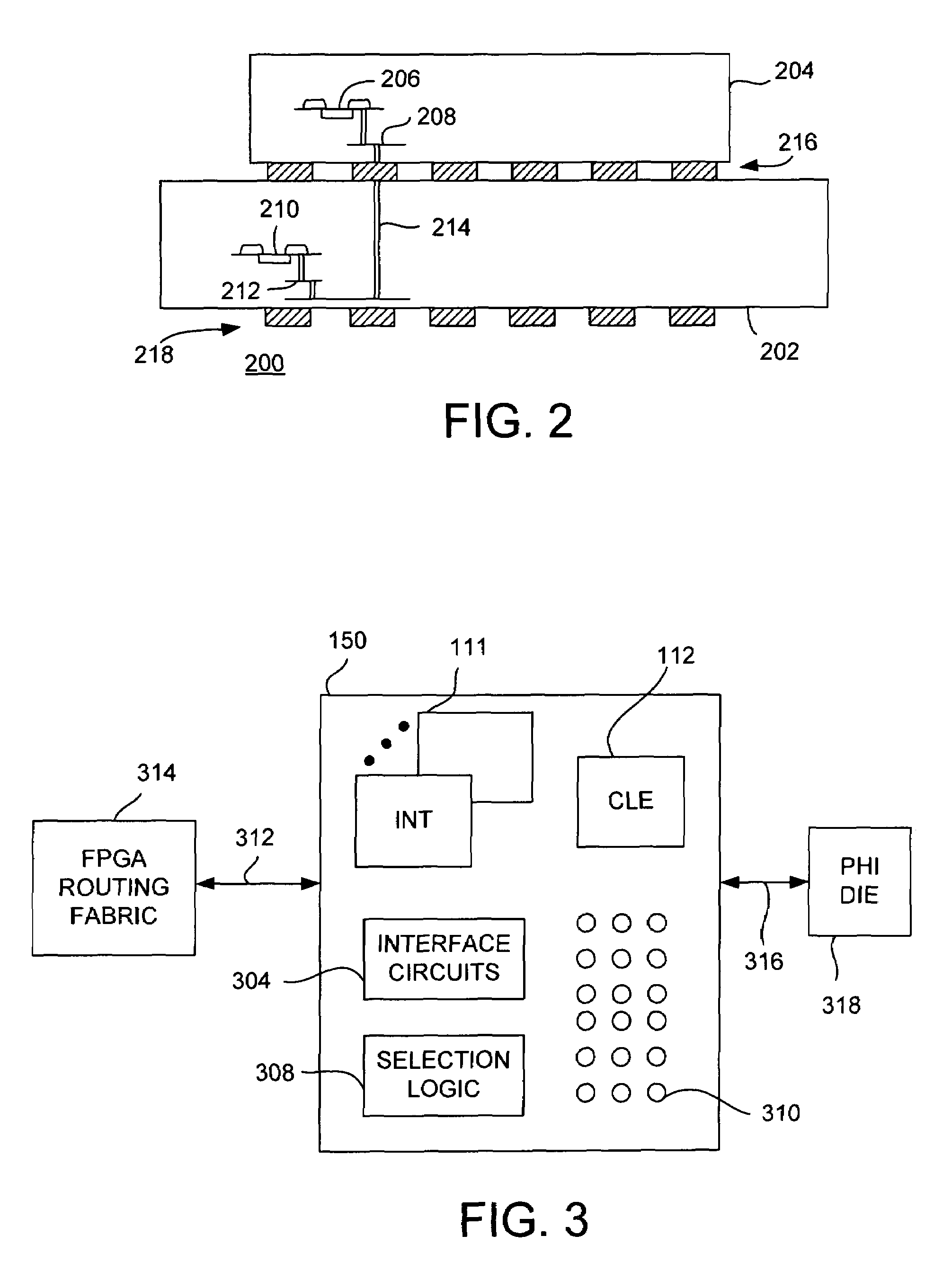
[0018]FIG. 1 is a block diagram depicting an exemplary embodiment of an FPGA 100 in accordance with one or more aspects of the invention. The FPGA 100 includes a large number of different programmable tiles including multi-gigabit transceivers (MGTs 101), configurable logic blocks (CLBs 102), random access memory blocks (BRAMs 103), input / output blocks (IOBs 104), configuration and clocking logic (CONFIG / CLOCKS 105), digital signal processing blocks (DSPs 106), specialized input / output blocks (I / O 107) (e.g., configuration ports and clock ports), and other programmable logic 108 such as digital clock managers, analog-to-digital converters, system monitoring logic, and so forth. Some FPGAs also include dedicated processor blocks (PROC 110). The FPGA 100 also includes one or more programmable heterogeneous integration (PHI) tiles 150. In some embodiments, the FPGA 100 includes a plurality of PHI tiles 150 arranged in a column. The PHI tiles 150 facilitate interconnection to one or mor...


PUM


Abstract

An integrated circuit with a through-die via (TDV) interface for die stacking is described. One aspect of the invention relates to an integrated circuit die having an array of tiles arranged in columns. The integrated circuit die includes at least one interface tile. Each interface tile includes a logic element, contacts, and through die vias (TDVs). The logic element is coupled to a routing fabric of the integrated circuit die. The contacts are configured to be coupled to conductive interconnect of another integrated circuit die attached to the backside of the integrated circuit die. The TDVs are configured to couple the logic element to the contacts.

Description

FIELD OF THE INVENTION[0001]One or more aspects of the present invention relate generally to semiconductor devices and, more particularly, to an integrated circuit with a through-die via (TDV) interface for die stacking.BACKGROUND OF THE INVENTION[0002]Programmable logic devices (PLDs) exist as a well-known type of integrated circuit (IC) that may be programmed by a user to perform specified logic functions. There are different types of programmable logic devices, such as programmable logic arrays (PLAs) and complex programmable logic devices (CPLDs). One type of programmable logic device, known as a field programmable gate array (FPGA), is very popular because of a superior combination of capacity, flexibility, time-to-market, and cost.[0003]An FPGA typically includes configurable logic blocks (CLBs), programmable input / output blocks (IOBs), and other types of logic blocks, such as memories, microprocessors, digital signal processors (DSPs), and the like. The CLBs, IOBs, and other ...

Claims


Application Information

Patent Timeline
Patent Type & Authority Patents(United States)
IPC IPC(8): H03K19/173
CPCH03K19/17796
Inventor RAHMAN, ARIFURTRIMBERGER, STEPHEN M.NEW, BERNARD J.
Owner XILINX INC
Why Eureka
Try Eureka