
Channel masking during integrated circuit testing

a technology of integrated circuits and masking, applied in the direction of electronic circuit testing, measurement devices, instruments, etc., can solve the problems of circuits that produce unknown responses, unpredictable final signatures, and exponential growth of signatures

Inactive Publication Date: 2009-04-21
CADENCE DESIGN SYST INC
View PDF8 Cites 50 Cited by
  • Summary
  • Abstract
  • Description
  • Claims
  • Application Information

AI Technical Summary

Benefits of technology

The patent describes a method for testing integrated circuits using a channel masking capability. This approach allows for masking out unknown or unpredictable values while avoiding problems caused by over-masking of known values. The circuitry added to the design is small and effective in masking unknown values during the testing process. The technical effect of this method is improved accuracy and efficiency in testing integrated circuits.

Problems solved by technology

One problem with compressing test responses into signatures is dealing with circuits that produce unknown responses.
An unknown response, if allowed to be captured into a signature register, will re-circulate, quickly making the final signature unpredictable.
However, when multiple unknown values are captured into a signature, the number of possible good signatures grows exponentially, and it quickly becomes impractical to predict all possible good response signatures.
However, the conventional methods lack the capability to mask out the specific channel bits containing unpredictable or unknown values.
When masking out the predictable values, over-masking occurs, and reduces the effectiveness of the test patterns.
For example, faults targeted by the test patterns may not be detected if the channel bit used to observe the fault's effect is masked due to over-masking.

Method used


Image

  • Channel masking during integrated circuit testing
  • Channel masking during integrated circuit testing
  • Channel masking during integrated circuit testing

Examples


Embodiment Construction

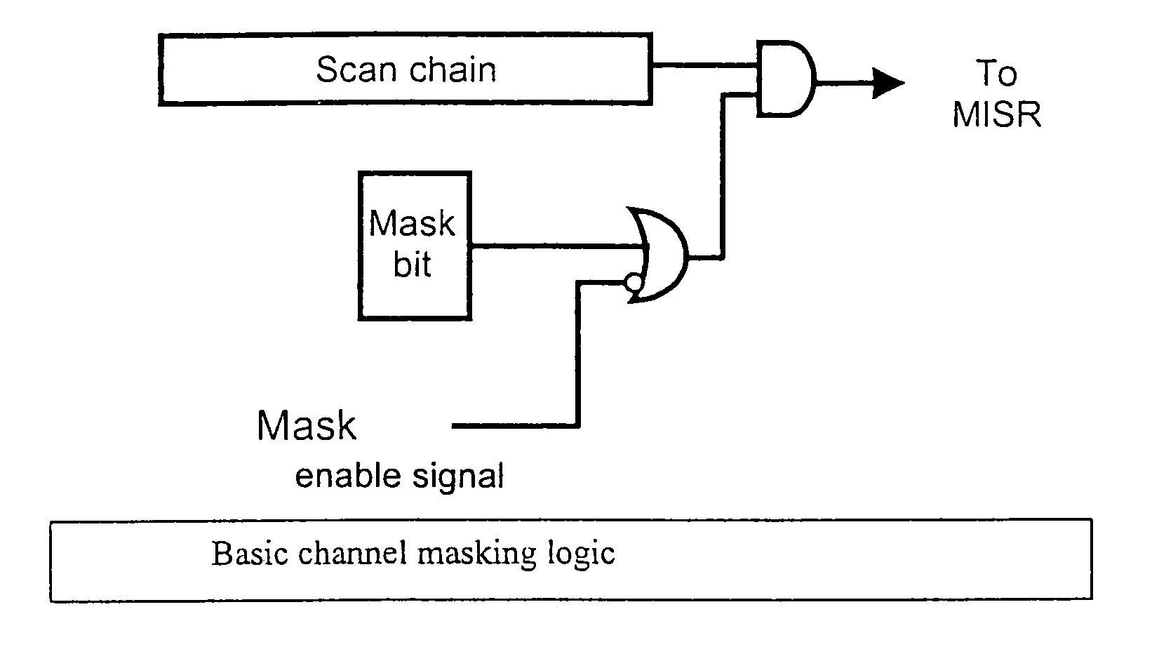
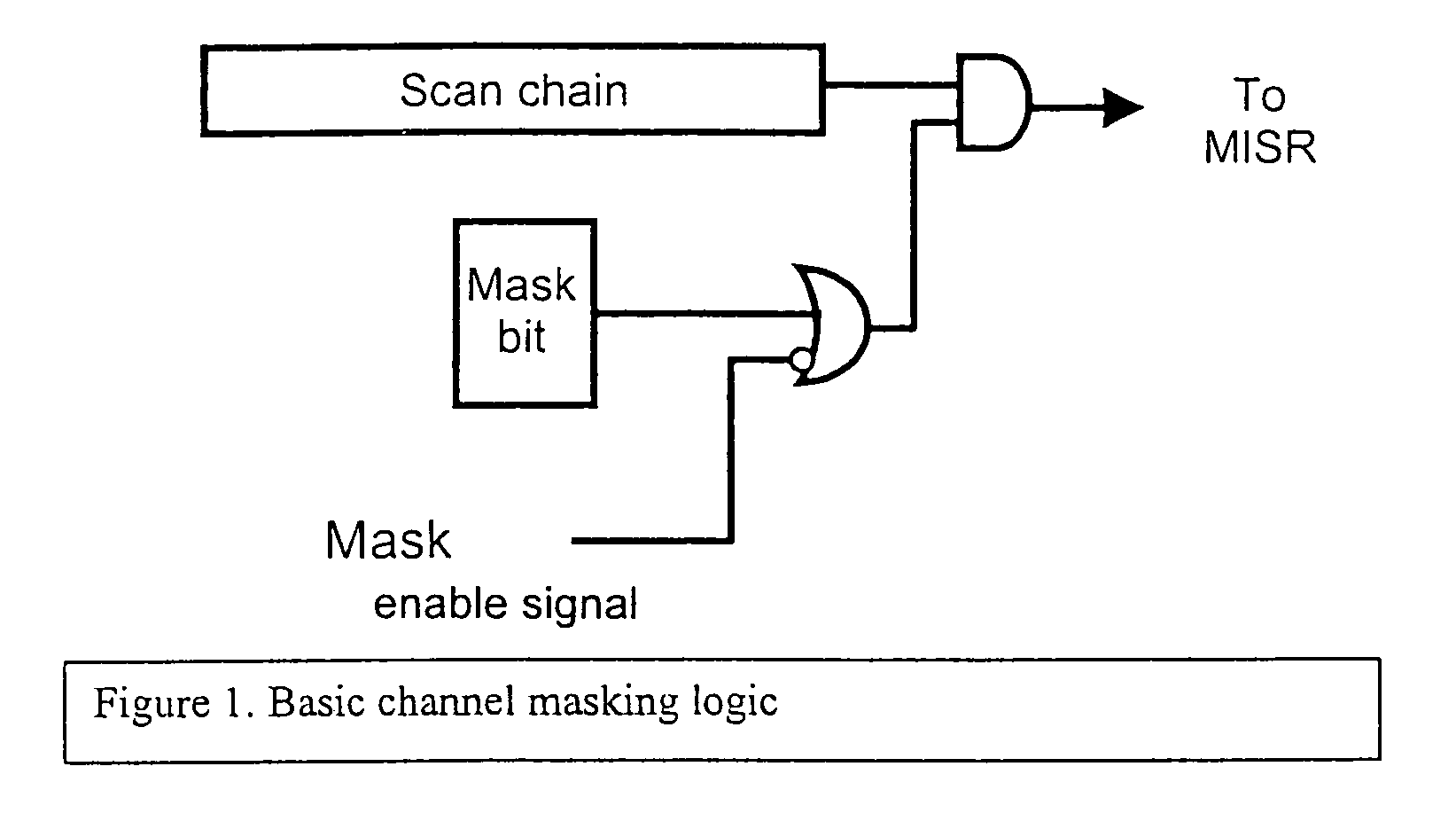
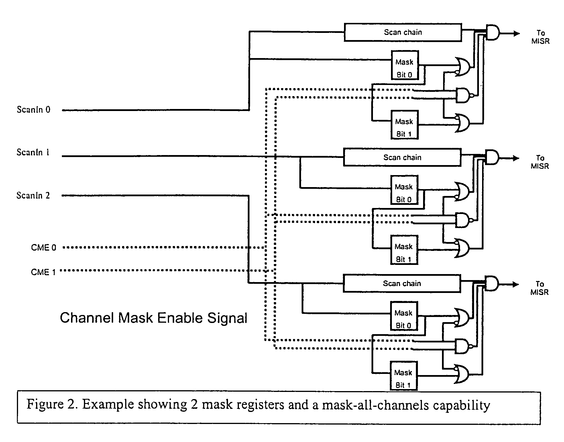
[0011]An integrated circuit whose scan chains, or channels, scan into a signature register, such as a multiple-input signature register (MISR) for example, during testing, uses a channel masking apparatus and method for masking unknown values that appear in response data when automatic test pattern generation test vectors are applied to the circuit, while minimizing the over-masking of known values. The channel masking method allows for multiple channel mask registers; provides an ability to load channel mask registers prior to scanning out the responses for a single test, so that each test can use an independent mask register state; and provides an ability to re-load the channel mask registers multiple times during the same scan-out process.

[0012]The channel mask registers may be loaded from a test bus of the scan-in pins, which can also be used to observe MISRs by making them bidirectional. The mask registers can be scan-loaded from this test bus either by using a scan clock separ...


PUM


Abstract

During testing of an integrated circuit (IC), a channel masking capability is used for masking out unknown or unpredictable (X) values from being compressed into a signature register. The approach provides flexibility to allow for masking of unknown values, while avoiding many of the problems caused by over-masking of known values. The circuitry added to the design to allow for masking is reasonably small, and provides an effective way of masking unknown values during the testing process.

Description

CROSS-REFERENCED AND RELATED APPLICATIONS[0001]This application claims the benefit of U.S. Provisional Application 60 / 503,191, filed on Sep. 15, 2003 which is hereby incorporated by reference as if fully set forth herein.BACKGROUND OF THE INVENTION[0002]Compression of test pattern response data into signatures is a well-established technique that has been used for decades, especially for logic built-in self-test (LBIST). More recently, it has been used as part of a more general approach for test data compression, in order to save data volume and test time.[0003]One problem with compressing test responses into signatures is dealing with circuits that produce unknown responses. An unknown response, if allowed to be captured into a signature register, will re-circulate, quickly making the final signature unpredictable. If just a single unknown value is captured, it is possible to predict two possible signatures, either of which could be assumed to be a non-defective response. However, ...

Claims


Application Information

Patent Timeline
Patent Type & Authority Patents(United States)
IPC IPC(8): G01R31/28
CPCG01R31/318547
Inventor KELLER, BRION
Owner CADENCE DESIGN SYST INC
Learn More