Bispectral multilayer photodiode detector and method for manufacturing such a detector

a photodiode detector and multi-layer technology, applied in the field of bispectral detection, can solve the problems of high surface recombination rate and many imperfections in the opening walls of the openings, and achieve the effect of avoiding pinching

Active Publication Date: 2012-03-22
COMMISSARIAT A LENERGIE ATOMIQUE ET AUX ENERGIES ALTERNATIVES
View PDF1 Cites 14 Cited by
  • Summary
  • Abstract
  • Description
  • Claims
  • Application Information

AI Technical Summary

Benefits of technology

[0068]In other words, this avoids pinch-off in the semiconductor zones of the second conductivity type in the upper layer due to the presence of the openings. T...

Problems solved by technology

However, regardless of the machining technology used to form openings 22, the walls of the openings always have many imperfecti...

Method used


Image

  • Bispectral multilayer photodiode detector and method for manufacturing such a detector
  • Bispectral multilayer photodiode detector and method for manufacturing such a detector
  • Bispectral multilayer photodiode detector and method for manufacturing such a detector

Examples


first embodiment

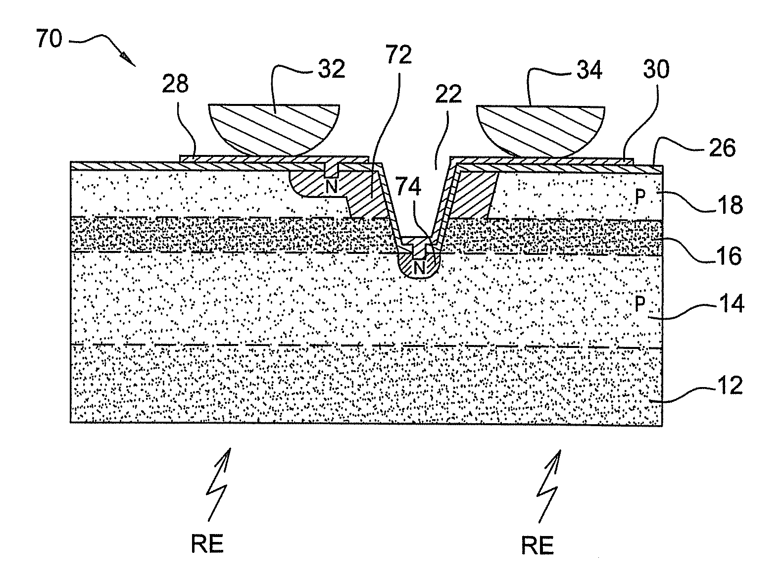
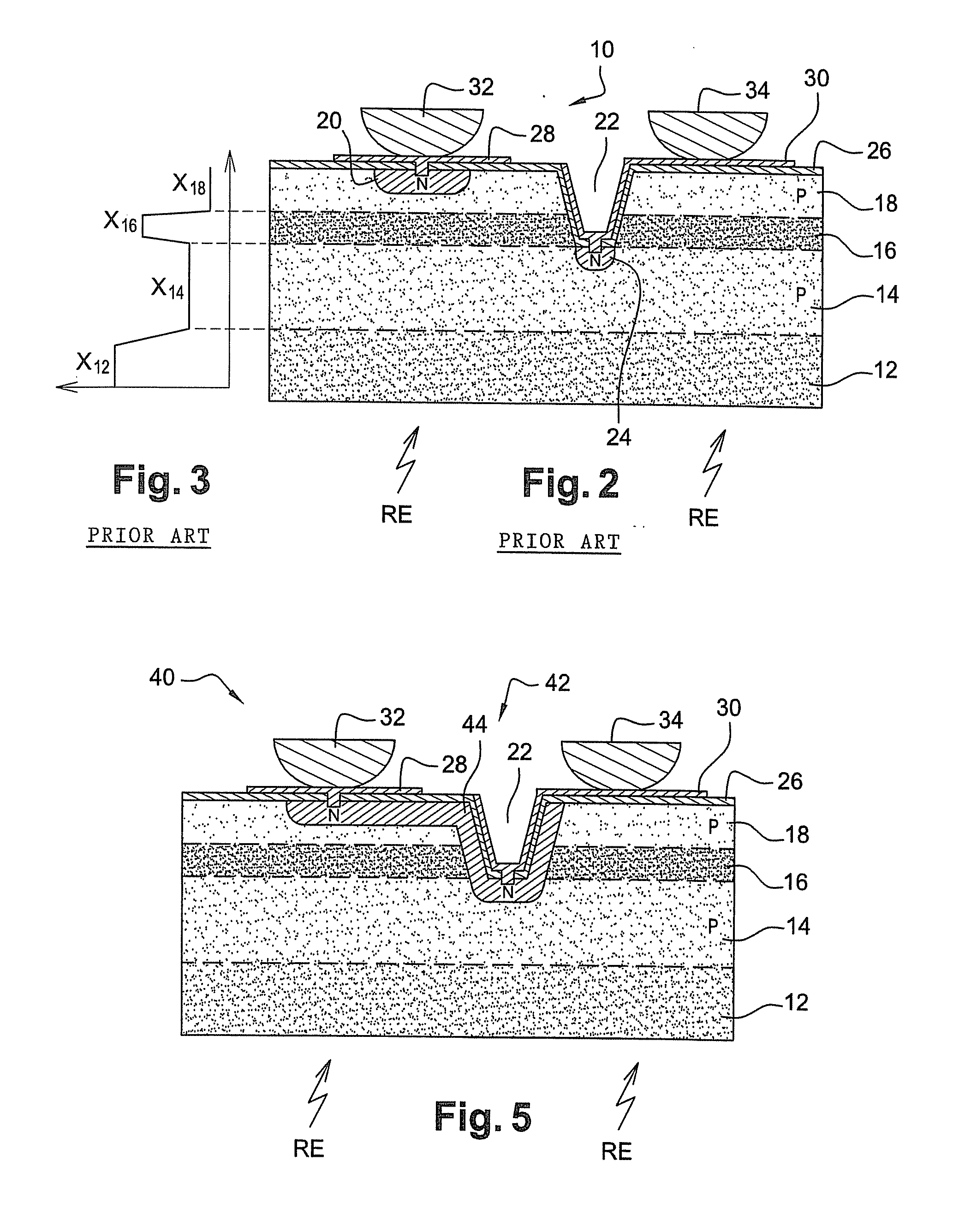
[0083]A detector 40 according to a first embodiment of the invention is described below making reference to FIGS. 3 and 6. Detector 40 differs from detector 10 in FIGS. 1 to 3 by virtue of the shape of the N-type semiconductor zones, or “N-type zones”, implanted in layers 14, 16 and 18 of the stack.

[0084]More especially, after depositing passivation layer 26, N-type doping is performed by boron ion implantation for example, on portions of the upper face 42 of the stack through passivation layer 26.

[0085]This ion implantation is preferably performed using an appropriate mask placed on the upper face 42 and masking the latter, except for those portions that are to be implanted. Layers 12, 14, 16, openings 22, contact pads 28, 30 and interfacing 32, 34 are produced in accordance with the method described in the document entitled “Status of HgCdTe bicolor and dual-band infrared array at LETI” by Destefanis, JEM 36(8), p. 1031, 2007.

[0086]Each of the implanted portions comprises an openi...

second embodiment

[0102]As stated earlier, the first embodiment makes it possible to optimise the fill factor of the photodiodes created by ion implantation. However, degraded performance may be observed because the N-type zones in upper layer 18 comprise vertical parts formed in the flanks of openings 22. There may be pinch-off regions in the PN junctions of upper layer 18, especially at locations where zone 44 forms a bend. Pinch-off in a PN junction has the effect of increasing the leakage currents in the latter, especially due to the tunnel effect.

[0103]In order to mitigate this problem, a detector 50 according to a second embodiment, shown in FIGS. 7 and 8 differs from the first embodiment in that N-type zones 20 of the upper layer, under contact pads 28, are distinct from the N-type zones 52 formed on the flanks of openings 22, as shown in FIGS. 7 and 8. N-type zones 20 of the PN junctions in upper layer 18 therefore do not contain any pinch-off region.

[0104]The method for fabricating detector ...

third embodiment

[0105]In the second embodiment, the potential of the N-type zones faulted on the flanks of openings 22 and contained in upper layer 18 is free to float because they are not connected to any fixed potential. The zones are electrically insulated from the zones in lower layer 14 because of the barrier function fulfilled by intermediate layer 16, as explained above in relation to the choice of materials used for the intermediate layer in the first embodiment, and are also not connected to the N-type zones of the PN junctions in upper layer 18 (which are brought to a potential for charge collection purposes).

[0106]If no bias is applied to the N-type zone on the flank of openings 22, the PN junction will naturally assume its open-circuit potential. However, because this potential floats, the space-charge zone of this PN junction is likely to fluctuate over time due to the effect of fluctuations in various parameters (e.g. fluctuation of the recombination current associated with the surfac...


PUM


Abstract

A bispectral detector comprising upper and lower semiconductor layers of a first conductivity type in order to absorb a first and a second electromagnetic spectrum, separated by an intermediate layer that forms a barrier; semiconductor zones of a second conductivity type implanted in upper layer and lower layer and each implanted at least partially in the bottom of an opening that passes through upper layer and intermediate layer; and conductor elements connected to semiconductor zones. At least that part of each opening that passes through upper layer is separated from the latter by a semiconductor cap layer: whereof the concentration of dopants of the second conductivity type is greater than 1017 cm−3; and whereof the thickness is chosen as a function of said concentration so that it exceeds the minority carrier diffusion length in the cap layer.

Description

FIELD OF THE INVENTION[0001]The invention relates to the field of bispectral detection using two absorption layers in a single stack in which PN junctions are formed.DESCRIPTION OF THE PRIOR ART[0002]A bispectral detector that is preferred because of its high fill factor and temporal coherence comprises a stack of several semiconductor layers for absorbing different electromagnetic radiation frequency ranges, the layers being insulated from each other and wherein PN junctions are formed in order to collect the charge carriers created by the absorption of incident radiation. Such a detector is described, for instance, in Document U.S. Pat. No. 6,034,407 and the document entitled “Status of HgCdTe bicolor and dual-band infrared array at LETI” by de Destefanis, Journal of Electronic Materials 36(8), p. 1031, (2007). These first two references relate to the material CdHgTe. An example of a similar structure using a different material can be consulted in the following document: Kim, “A T...

Claims


Application Information

Patent Timeline
IPC IPC(8): H01L31/0352
CPCH01L27/14641H01L27/14652Y02E10/50H01L31/11H01L31/1832H01L27/14696H01L31/1013
Inventor GRAVRAND, OLIVIERBAYLET, JACQUES
Owner COMMISSARIAT A LENERGIE ATOMIQUE ET AUX ENERGIES ALTERNATIVES
Why Eureka
Try Eureka