Bipolar transistor having a low doped drift layer of crystalline SiC

a crystalline sic, low-drift layer technology, applied in the direction of transistors, electrical devices, semiconductor devices, etc., can solve the problems of low emitter injection efficiency, high control current that must be supplied to the contact for the base of the transistor, and thin base layer suffer from punch-through breakdown

Inactive Publication Date: 2001-11-06
CREE INC
View PDF4 Cites 37 Cited by
  • Summary
  • Abstract
  • Description
  • Claims
  • Application Information

AI Technical Summary

Benefits of technology

It has been found that the introduction of such a first layer of such a wider bandgap material will make it possible to reduce the on-state losses of the transistor by making it possible to obtain the on-state of the transistor by using a lower base current than would be necessary for a bipolar transistor with all the layers made of the same semiconductor material of crystalline siC.
According to a first preferred embodiment of the invention the emitter of the transistor is one said first layer. This results in a heterojunction between the emitter and the base, and this heterojunction will maintain a high carrier injection from the emitter through a low barrier therefore and suppresses the carrier injection from the base thanks to an increased valence band barrier against such injection, even with high base doping, solving the problem of a high base doping in an ordinary bipolar transistor resulting in a low emitter injection efficiency and an increased base control current.
According to another preferred embodiment of the invention said means are formed by a sub-layer of said base layer located next to said contact electrode and having a higher doping concentration of said first conductivity type than the rest of the base layer, and a further preferred embodiment of the invention has said means formed by the arrangement of one said first layer next to the base layer for forming the base layer contact electrode and which is doped according to the first conductivity type, so that the energy barrier for the minority charge carriers will in the first case be formed by said higher doping concentration and in the second case by the introduction of a heterojunction at the base contact, and both measures will efficiently decrease electron re-combination at the base contact.
According to another preferred embodiment of the invention the base of the transistor is formed by a grid doped according to a first conductivity type and buried in the drift layer doped according to an opposite, second conductivity type while leaving drift layer regions between adjacent grid bars, the emitter and the collector of the transistor being also doped according to said second conductivity type. A bipolar transistor with this totally new design will also have the on-state losses efficiently reduced. This is mainly achieved by the fact that the charge carriers injected into the drift layer from the emitter has not to be transported in any layer in which they are minority charge carriers, which means a longer life time of the charge carriers. It will also be possible to obtain the plasma in the drift layer at a lower current of charge carriers of the first conductivity type, so that the base control current needed for obtaining a low collector-emitter voltage will be reduced. This means in the case of an emitter of n-type and accordingly a base layer of p-type that the electrons injected from the emitter have not to be transported through a p-doped region and possible limitations of very low life-times in the highly doped p-base of standard HBT due to re-combination central in e.g. B- and Al-doped SiC, are avoided, and the plasma may be obtained at a lower hole current supplied through the grid.
According to another preferred embodiment of the invention being a further development of the embodiment last mentioned the transistor comprises two base grids, one arranged close to the emitter and the other close to the collector, so that the transistor is bi-directional with respect to current conduction and turn-off capabilities and the base grid closest to the emitter in the respective type of operation of the transistor is arranged to be used to control the transistor. Accordingly, this will make the operation of the transistor more flexible and broaden the possible applications thereof. There will also be a possibility of an increased injection of holes from the anode-side of the diode, which will give a further reduction of the on-state losses.
According to another preferred embodiment of the invention the base grid is one said first layer. This will reduce the base current needed for obtaining the low on-state voltage aimed at, and so will the design of the emitter as one said first layer, and it is particularly advantageous that both the base grid and the emitter are a said first layer of a material having a wider energy gap between the conduction band and the valence band than the SiC of the drift layer, which reduces the base current needed for a low collector-emitter voltage drastically, well by more than an order of magnitude.

Problems solved by technology

This type of transistor already known is normally called Bipolar Junction Transistor (BJT) and a major drawback of such transistors already known for high power applications is the high control current that must be supplied to the contact for the base of the transistor.
To achieve a low control current the base width must be very small, but a thin base layer suffers from punch-through breakdown unless the doping is high.
A high base doping lowers the emitter injection efficiency and this increases the control current.
This means in practice that a high control current must be supplied to the base contact in the on-state of the transistor resulting in unnecessarily and mostly unacceptably high power losses.
It has been found that it is not possible to achieve full benefit of the HBT-structure with an heterojunction between the emitter and the base without solving the problem of recombination of minority charge carriers at the base contact.
If this is not done the benefits of the HBT-structure may be lost, since a great part of the minority charge carriers injected into the base layer from the emitter will be "absorbed" by the base contact through re-combination with opposite charge carriers.
However, this problem is solved by the introduction of said means forming an energy barrier for the minority charge carriers resulting in a diversion of such charge carriers coming close to the base contact in the direction of the collector instead.

Method used


Image

  • Bipolar transistor having a low doped drift layer of crystalline SiC
  • Bipolar transistor having a low doped drift layer of crystalline SiC
  • Bipolar transistor having a low doped drift layer of crystalline SiC

Examples


Embodiment Construction

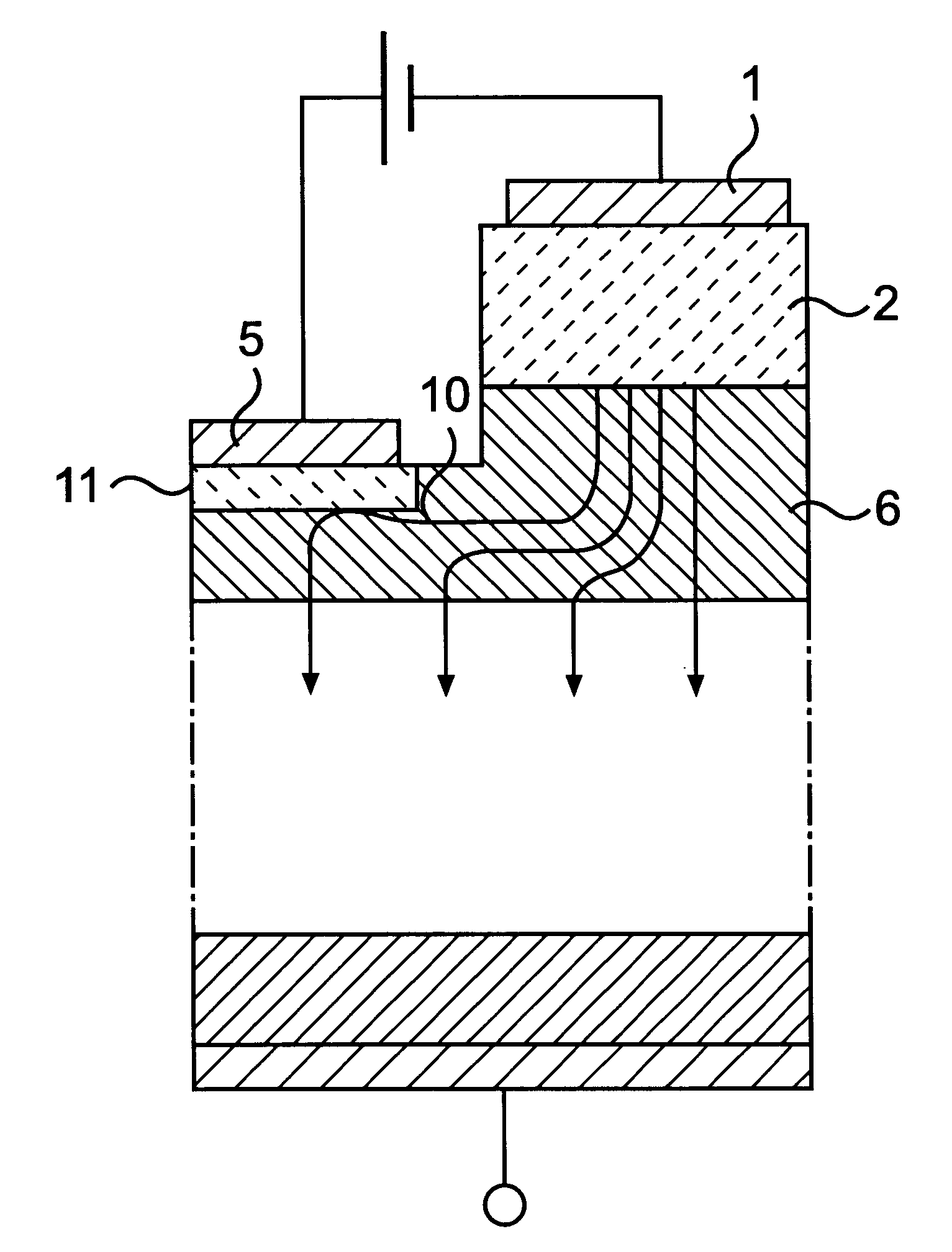
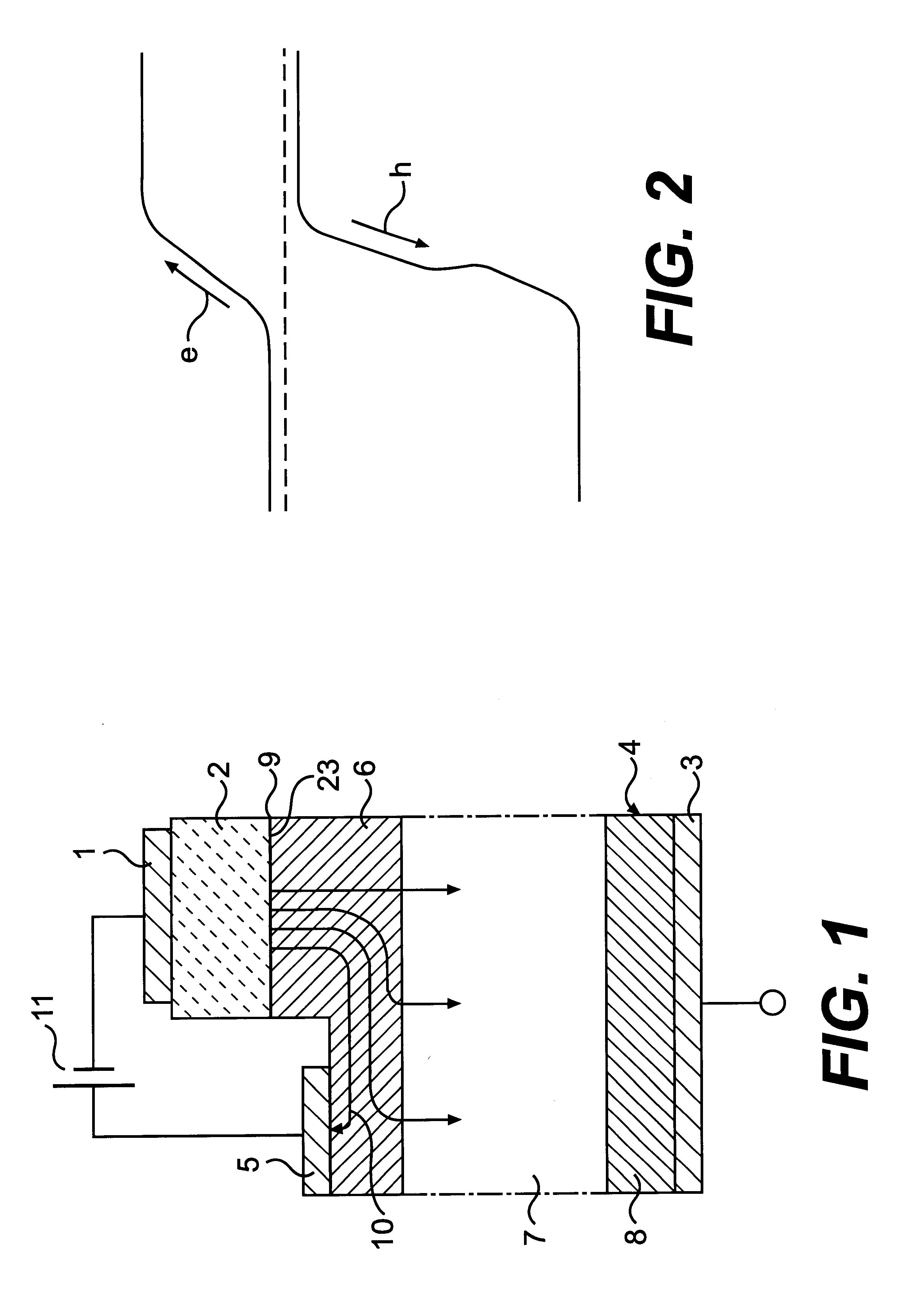
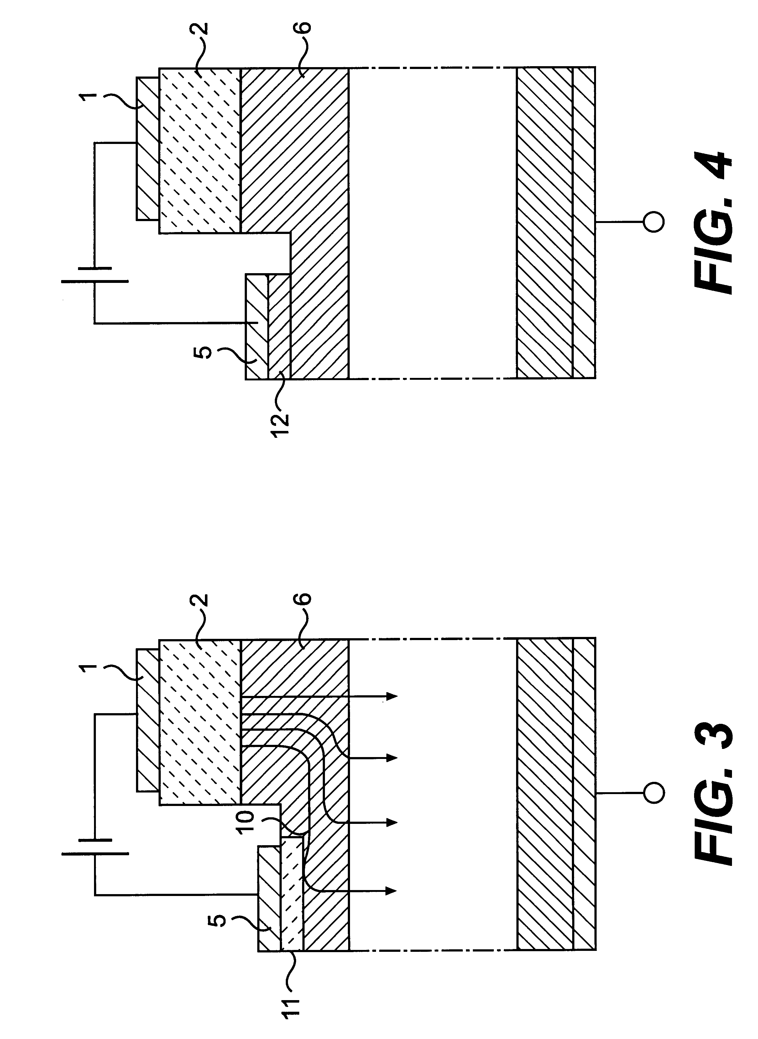
A Heterojunction Bipolar Transistor made of SiC, for instance of the 4H-polytype, is schematically illustrated in FIG. 1. However, it should be noticed that the relative dimensions of the regions in this device shown in this figure and also in the other figures have only been chosen for the sake of clearness of the drawing.

This transistor has three electrodes, namely one electrode 1 making contact to an emitter 2, an electrode 3 making contact to a collector 4 and an electrode 5 making contact to a base 6. The emitter 2 is doped according to a first conductivity type, and this first conductivity type will hereinafter be considered to be n-type throughout the description, but it is emphasized that it will be possible to exchange the conductivity types of all layers in all different embodiments to the opposite. In obtaining numerical values shown in FIGS. 5 and 7 following typical values of dopings and layer thicknesses were used for the sake of illustration. The doping concentration ...


PUM


Abstract

A bipolar transistor having at least a low doped drift layer (14) of crystalline SiC comprises at least one first layer (13) of a semi-conductor material having a wider energy gap between the conduction band and the valence band than an adjacent layer (14) of SiC.

Description

FIELD OF THE INVENTION AND PRIOR ARTThe present invention relates to a bipolar transistor having at least a low doped drift layer of crystalline SiC.SiC has some excellent physical properties, such as a high thermal stability, a high thermal conductivity and especially a high breakdown field being approximately ten times higher than for Si, which makes SiC well suited as a material for high power devices operating under conditions were high voltages may occur in the blocking state of the device. The high breakdown field makes it possible to make transistors of SiC comparatively thin and still able to hold high voltages in the blocking state thereof reducing on-state losses.The present invention is particularly occupied with bipolar transistors for high power applications, specifically in the fields of distribution and transmission of electric energy, for example in converters of different types as in HVDC converter stations, and will hereinafter be explained with respect thereto, bu...

Claims


Application Information

Patent Timeline
Patent Type & Authority Patents(United States)
IPC IPC(8): H01L29/66H01L29/739H01L29/737H01L29/02H01L29/24H01L21/331H01L29/10H01L29/20H01L29/267H01L29/732
CPCH01L29/1004H01L29/267H01L29/7371H01L29/739H01L29/1608H01L29/2003
Inventor BAKOWSKI, MIETEKBREITHOLTZ, BOGUSTAFSSON, ULFZDANSKY, LENNART
Owner CREE INC
Why Eureka
Try Eureka