Integrated process modulation (IPM) a novel solution for gapfill with HDP-CVD

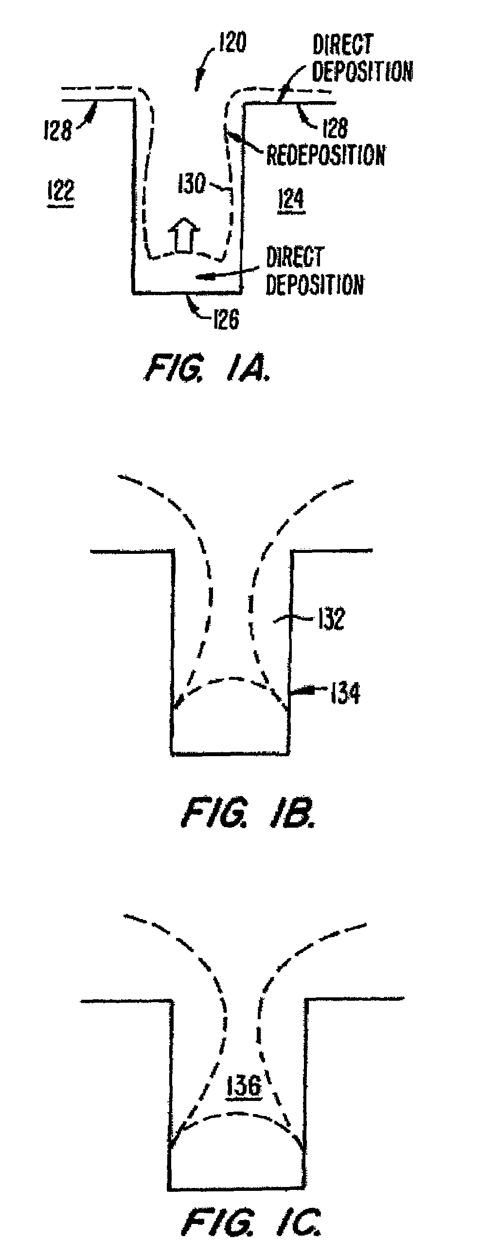
a technology of integrated process and cvd, which is applied in the field of integrated process modulation (ipm) a novel solution for gapfill with hdp-cvd, can solve the problems of difficult to fill spaces using conventional cvd methods, increased aspect ratio gaps in some applications, and limited sputtering angular redistribution of sputtered materials, so as to reduce moisture in the layer and prevent the effect of attack

Inactive Publication Date: 2009-04-28
APPLIED MATERIALS INC
View PDF110 Cites 49 Cited by
  • Summary
  • Abstract
  • Description
  • Claims
  • Application Information

AI Technical Summary

Benefits of technology

[0017]The method may optionally comprise depositing the layer by cooling the substrate to less than 400° C., and after repeating the depositing-etching cycle the predetermined number of cycles, heating the substrate to reduce moisture in the layer. In some embodiments, the method may comprise, before initiating the depositing-etching cycle, seasoning the chamber with a silicon-rich deposit to prevent attack of the chamber by etching gases used in etching the portion of the layer (e.g., with a seasoning deposition in the chamber that is 4 to 20 times thicker than a deposition thickness of a single layer).

Problems solved by technology

Smaller feature sizes have resulted in the presence of increased aspect ratio gaps for some applications, for example, between adjacent conductive lines or in etched trenches.
These spaces are difficult to fill using conventional CVD methods.
However, a limitation associated with sputtering is an angular redistribution of sputtered material.
For example, in an STI gapfill, the sputtered SiO2 can be sputtered from above the trench and deposit on the sides of the trench, causing excess buildup, and limiting the opening through which bottom-up gapfill is achieved.
If there is too much re-deposition, the trench can close off before the bottom is filled, leaving a buried void within the trench.
With tighter trenches, the risk of closing the trench before the bottom-up fill is complete becomes greater, even with the lighter atoms.
Spin-on dielectric and ALD (atomic layer deposition) films have shown gapfill capabilities down to much tighter structures than HDP-CVD has been able to fill, but customers are somewhat reluctant to make the switch for other reasons such as film shrinkage and reliability.
A disadvantage of conventional DED processes with separately tuned processes for each deposition and etch step is that each step generally needs to be separately qualified in manufacturing.

Method used


Image

  • Integrated process modulation (IPM) a novel solution for gapfill with HDP-CVD
  • Integrated process modulation (IPM) a novel solution for gapfill with HDP-CVD
  • Integrated process modulation (IPM) a novel solution for gapfill with HDP-CVD

Examples


Embodiment Construction
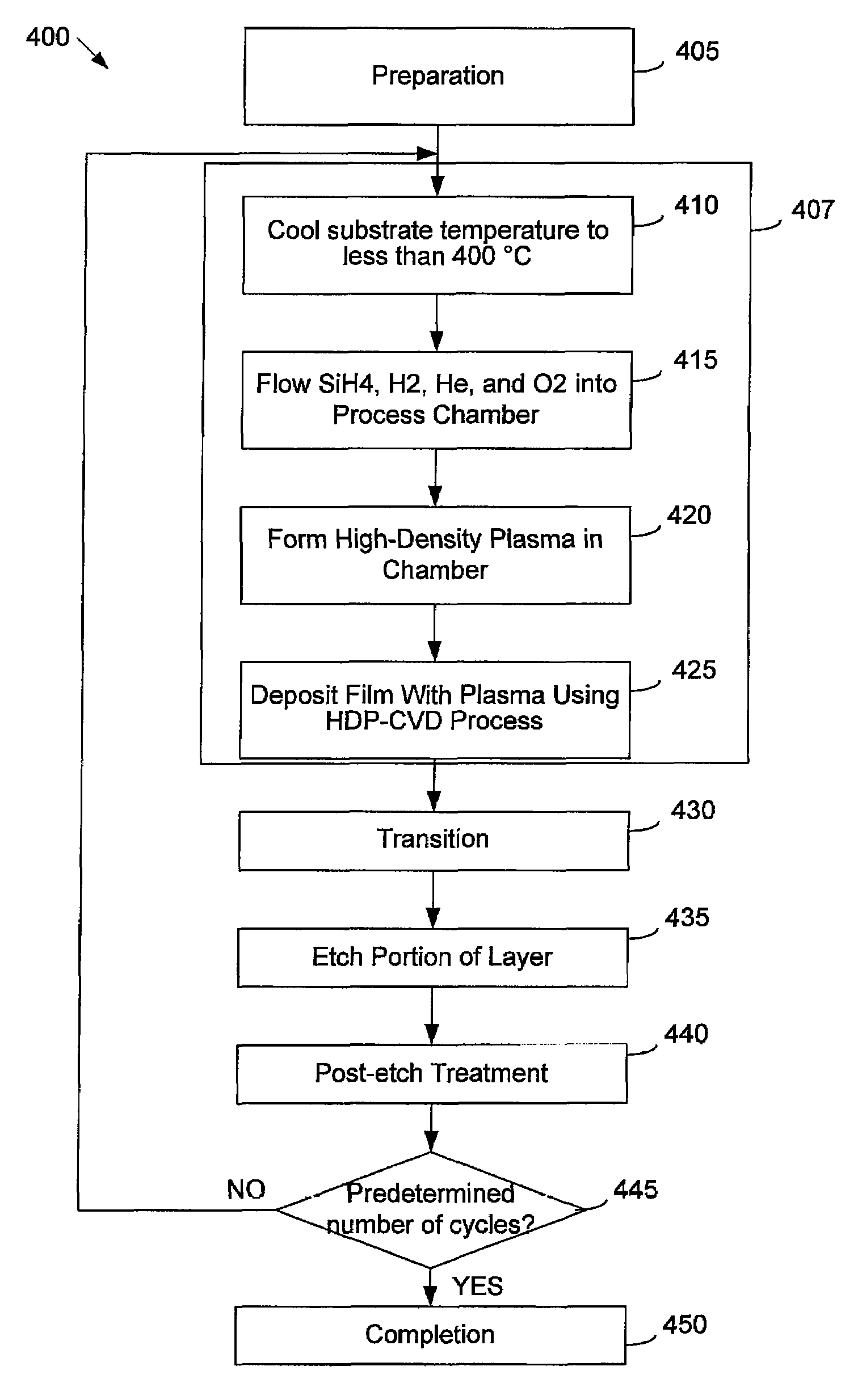
[0024]Introduction

[0025]Embodiments of the invention pertain to a high-density-plasma chemical-vapor-deposition (“HDP-CVD”) method applicable, for example, to depositing layers in shallow trench isolation (“STI”) applications. Embodiments of the invention permit material to be deposited with substantially 100% gapfill for integrated circuits having small feature sizes (90 nm or less). Bottom-up gapfill may be achieved inside very aggressive trenches having high aspect ratios.

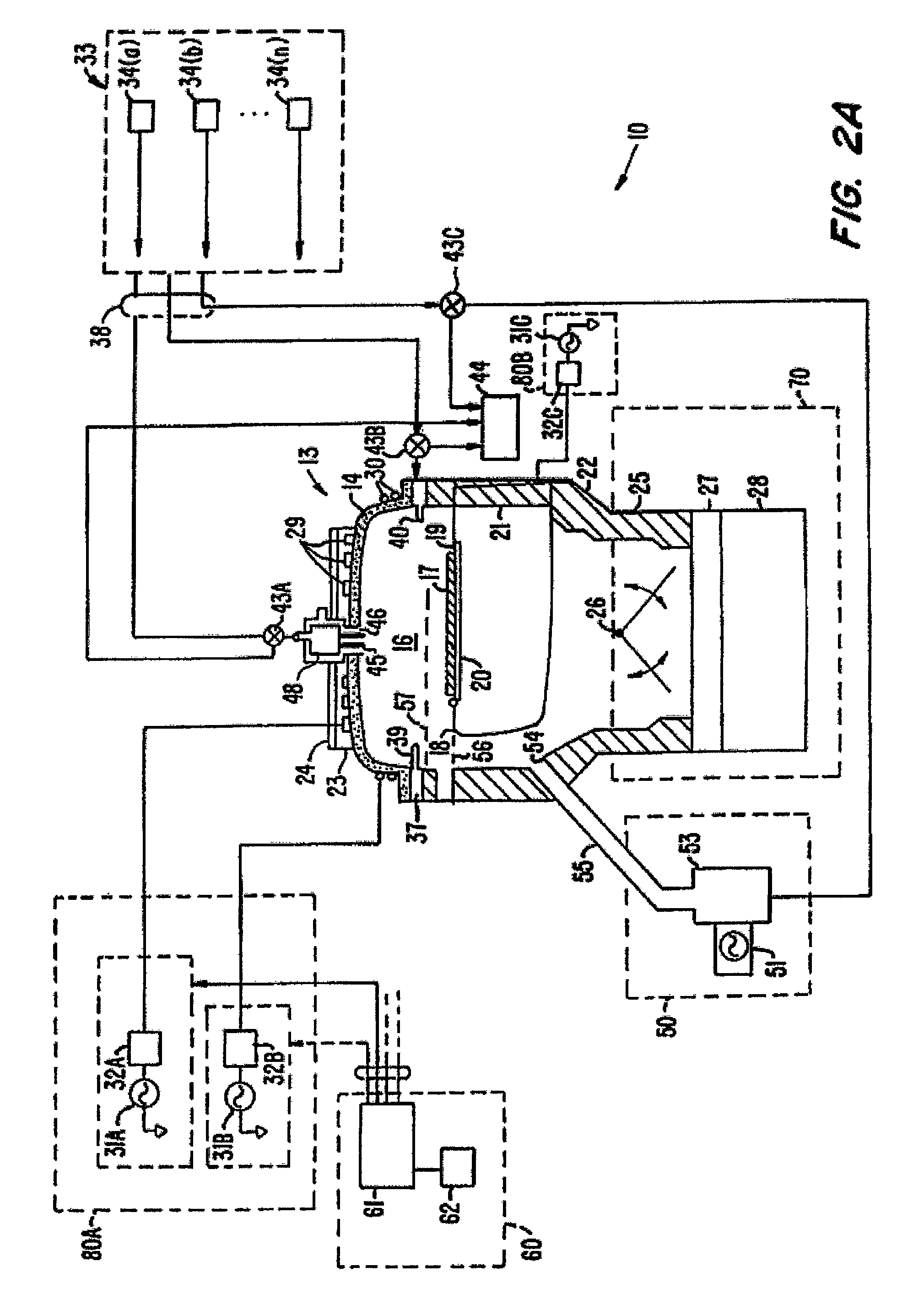
[0026]Embodiments of the present invention can be implemented using a variety of high density plasma CVD substrate processing chambers including chambers in which a plasma is formed by the application of RF energy to a coil that at least partially surrounds a portion of the chamber and chambers that use ECR plasma formation techniques. An example of an inductively-coupled HDP-CVD chamber in which embodiments of the method of the present invention can be practiced is set forth below.

[0027]Exemplary Substrate Proc...


PUM


Abstract

A process is provided for depositing an silicon oxide film on a substrate disposed in a process chamber. A process gas that includes a halogen source, a fluent gas, a silicon source, and an oxidizing gas reactant is flowed into the process chamber. A plasma having an ion density of at least 1011 ions / cm3 is formed from the process gas. The silicon oxide film is deposited over the substrate with a halogen concentration less than 1.0%. The silicon oxide film is deposited with the plasma using a process that has simultaneous deposition and sputtering components. The flow rate of the halogen source to the process chamber to the flow rate of the silicon source to the process chamber is substantially between 0.5 and 3.0.

Description

CROSS-REFERENCE TO RELATED APPLICATIONS[0001]This application claims priority to U.S. Provisional Patent Application No. 60 / 792,743, filed Apr. 17, 2006, entitled “INTEGRATED PROCESS MODULATION (IPM) A NOVEL SOLUTION FOR FILLING NARROW GAPS (<90 NM) WITH HDP-CVD-S,” the entire disclosure of which is incorporated herein by reference for all purposes.BACKGROUND OF THE INVENTION[0002]One of the primary steps in the fabrication of modern semiconductor devices is the formation of a film, such as a silicon oxide, on a semiconductor substrate. Silicon oxide is widely used as an insulating layer in the manufacture of semiconductor devices. As is well known, a silicon oxide film can be deposited by thermal chemical vapor deposition (CVD) or a plasma chemical vapor deposition process, among other techniques. In a conventional thermal CVD process, reactive gases are supplied to the substrate surface where heat-induced chemical reactions (homogeneous or heterogeneous) take place to produce a...

Claims


Application Information

Patent Timeline
Patent Type & Authority Patents(United States)
IPC IPC(8): H01L21/20
CPCH01L21/76224H01L21/02164H01L21/02274H01L21/31116H01J37/32495C23C16/401C23C16/045C23C16/50C23C16/56
Inventor NEMANI, SRINIVAS D.LEE, YOUNG S.YIEH, ELLIE Y.WANG, ANCHUANBLOKING, JASON THOMASHAN, LUNG-TIEN
Owner APPLIED MATERIALS INC
Why Eureka
Try Eureka