Unlock instant, AI-driven research and patent intelligence for your innovation.

Semiconductor device and methods of manufacturing the same

a semiconductor and semiconductor technology, applied in semiconductor devices, digital storage, instruments, etc., to achieve the effect of preventing a threshold voltage of the non-selected transistor from being increased

Active Publication Date: 2009-04-28
SAMSUNG ELECTRONICS CO LTD
View PDF6 Cites 0 Cited by
  • Summary
  • Abstract
  • Description
  • Claims
  • Application Information

AI Technical Summary

Benefits of technology

This solution effectively suppresses gate disturbance, ensuring that only the selected cell is programmed without influencing adjacent cells, improving operational characteristics and reliability of the semiconductor device.

Problems solved by technology

However, when the unit cells having the single-poly EEPROM structure are arrayed, the hot electrons excessively generated in programming the cell are moved into an adjacent cell so that they become trapped in an adjacent floating gate electrode.

Method used


Image

  • Semiconductor device and methods of manufacturing the same
  • Semiconductor device and methods of manufacturing the same
  • Semiconductor device and methods of manufacturing the same

Examples


Embodiment Construction

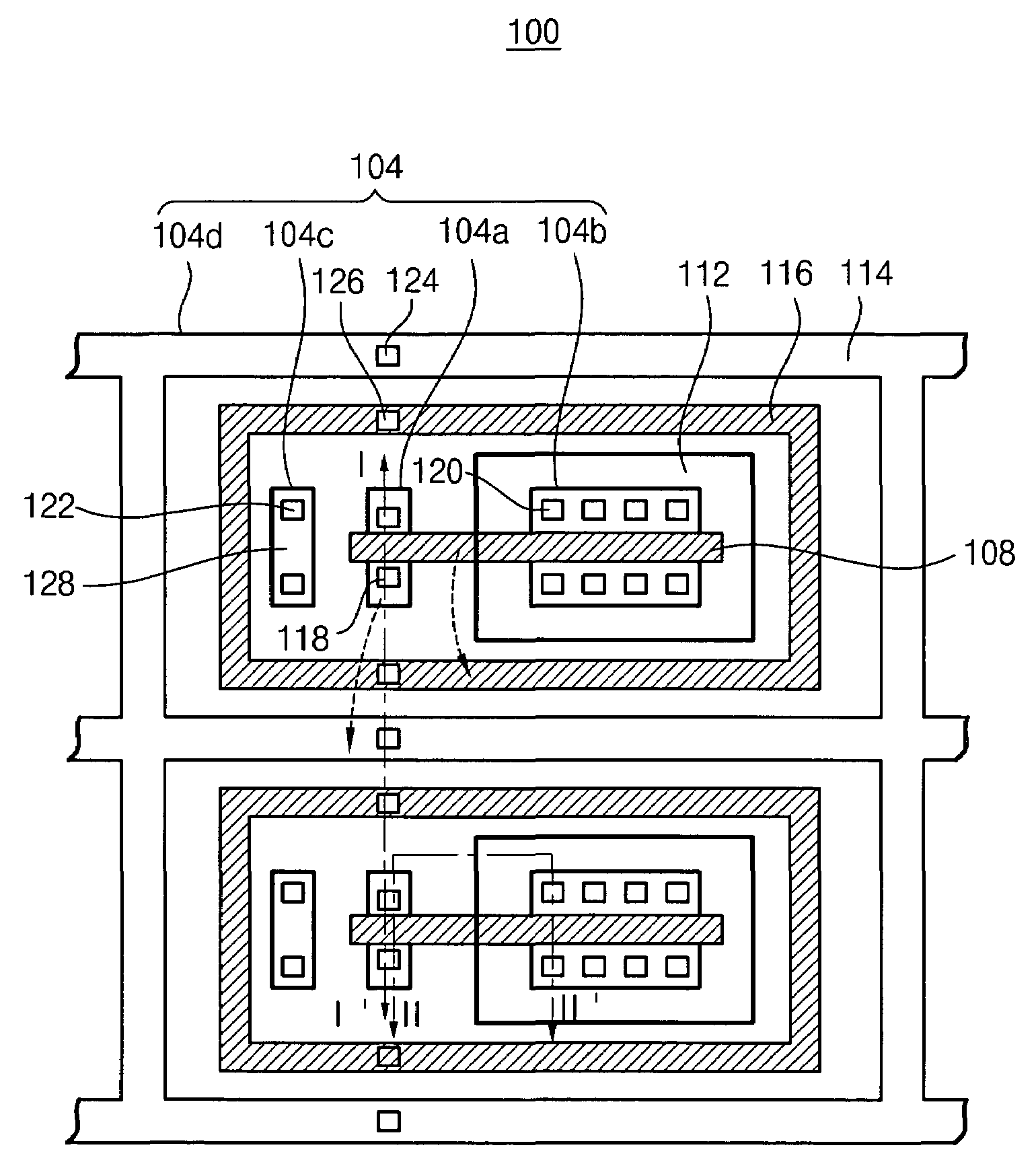
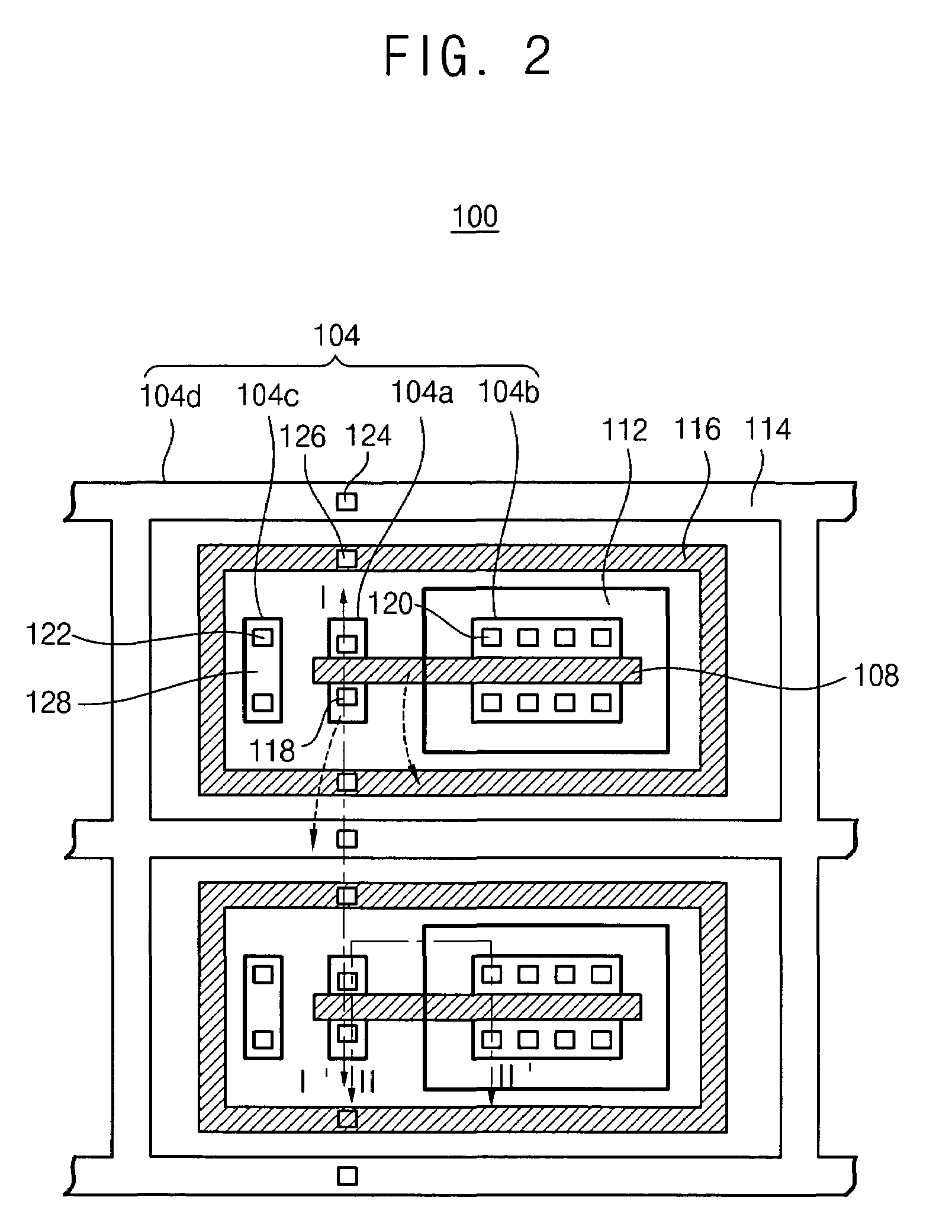
[0032]The exemplary embodiments of the present invention are described more fully hereinafter with reference to the accompanying drawings, in which embodiments of the invention are shown. This invention may, however, be embodied in many different forms and should not be construed as limited to the embodiments set forth herein. In the drawings, the sizes and relative sizes of layers and regions may be exaggerated for clarity.

[0033]It will be understood that when an element or layer is referred to as being “on”, “connected to” or “coupled to” another element or layer, it can be directly on, connected or coupled to the other element or layer or intervening elements or layers may be present. In contrast, when an element is referred to as being “directly on,”“directly connected to” or “directly coupled to” another element or layer, there are no intervening elements or layers present. Moreover, the term “heavily doped” as used herein refers to a higher than average concentration of doping...


PUM


Abstract

A semiconductor device includes at least two transistors and a charge-trapping structure. The charge-trapping structure traps charges, which are moved from a selected transistor toward a non-selected transistor, adjacent to the selected transistor among the transistors, thereby preventing a threshold voltage of the non-selected transistor from being increased. Thus, the charge-trapping structure traps the charges so that an increase of the threshold voltage of the non-selected voltage is suppressed.

Description

CROSS REFERENCE TO RELATED APPLICATION[0001]This application claims priority under 35 USC § 119 to Korean Patent Application No. 2004-94891, filed on Nov. 19, 2004, the contents of which are herein incorporated by reference in its entirety for all purposes.BACKGROUND OF THE INVENTION[0002]1. Field of the Invention[0003]The present invention relates to a semiconductor device and to methods of manufacturing the semiconductor device. More particularly, the present invention relates to a non-volatile memory device that is capable of being programmed once, and to methods of manufacturing the non-volatile memory device.[0004]2. Description of the Related Art[0005]Recently, the demand for liquid crystal display (LCD) driver integrated circuit (IC) (hereinafter referred to as an LDI) mobile devices has greatly increased. To reduce manufacturing costs, the LDI, a COM and SEG driver circuit and a power circuit have been integrated into a single chip. Also, two CMOS (Complementary Metal Oxide ...

Claims


Application Information

Patent Timeline
Patent Type & Authority Patents(United States)
IPC IPC(8): G11C16/04H10B69/00
CPCG11C16/18G11C17/146H01L27/115H01L27/11521H01L27/11558H10B69/00H10B41/30H10B41/60
Inventor LEE, SOO-CHEOLLEE, KI-JIK
Owner SAMSUNG ELECTRONICS CO LTD