Apparatus for fixed-form multi-planar extension of electrical conductors beyond the margins of a substrate

a technology of multi-planar extension and apparatus, which is applied in the direction of electronic circuit testing, measurement devices, instruments, etc., can solve the problems of poor signal integrity, poor overall dimensional accuracy, and inability to package integrated circuits that cannot perform as desired, etc., and achieve the effects of reducing the cost of manufacturing, and improving the accuracy of measuremen

Active Publication Date: 2009-05-12
TRANSLARITY INC
View PDF13 Cites 15 Cited by
  • Summary
  • Abstract
  • Description
  • Claims
  • Application Information

AI Technical Summary

Problems solved by technology

In this way, integrated circuits that cannot perform as desired are not packaged, or otherwise incorporated into finished products.
The maintenance of probe tip accuracy, good signal integrity, and overall dimensional accuracy severely strains even the best of these highly developed fabrication methods because of the multiple component and assembly error budget entries.

Method used


Image

  • Apparatus for fixed-form multi-planar extension of electrical conductors beyond the margins of a substrate
  • Apparatus for fixed-form multi-planar extension of electrical conductors beyond the margins of a substrate
  • Apparatus for fixed-form multi-planar extension of electrical conductors beyond the margins of a substrate

Examples


Embodiment Construction

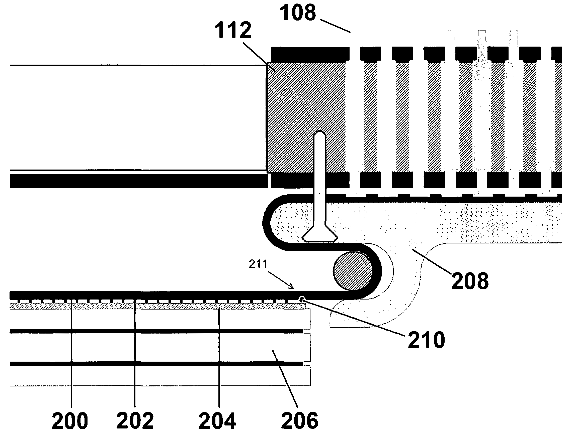
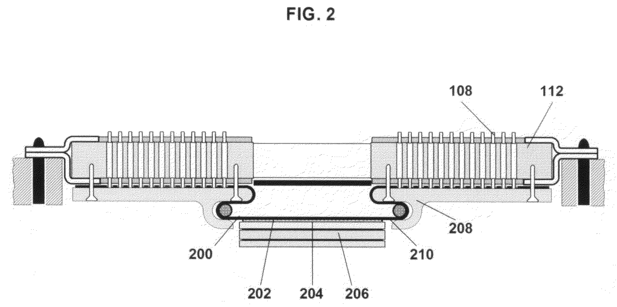
[0019]Generally, an apparatus provides electrical pathways between pads of unsingulated integrated circuits and pogo pins disposed in a pogo tower of a semiconductor test system without the need of a probe card.

[0020]Reference herein to “one embodiment”, “an embodiment”, or similar formulations, means that a particular feature, structure, operation, or characteristic described in connection with the embodiment, is included in at least one embodiment of the present invention. Thus, the appearances of such phrases or formulations herein are not necessarily all referring to the same embodiment. Furthermore, various particular features, structures, operations, or characteristics may be combined in any suitable manner in one or more embodiments.

Terminology

[0021]Reference herein to “circuit boards”, unless otherwise noted, is intended to include any type of substrate upon which circuits may be placed. For example, such substrates may be rigid or flexible, ceramic, flex, epoxy, FR4, or any...


PUM


Abstract

An apparatus, suitable for coupling a pads of integrated circuits on wafer to the pogo pins of a pogo tower in a test system without the need of a probe card, includes a body having a first surface and a second surface, the body having a substantially circular central portion, and a plurality of bendable arms extending outwardly from the central portion, each bendable arm having a connector tab disposed at the distal end thereof; a first plurality of contact terminals disposed on the second surface of the central portion of the body, the first plurality of contact terminals arranged in pattern to match the layout of pads on a wafer to be contacted; at least one contact terminal disposed on the first surface of the plurality of connector tabs; and a plurality of electrically conductive pathways disposed in the body such that each of the first plurality of contact terminals is electrically connected to a corresponding one of the contact terminals on the first surface of the connector tabs.

Description

CROSS-REFERENCE TO RELATED APPLICATION[0001]This non-provisional application claims the benefit of provisional application 60 / 812,156, filed 9 Jun. 2006, and entitled “Method And Apparatus For Fixed-Form Multi-Planar Extension Of Electrical Conductors Beyond The Margins Of A Substrate”, the entirety of which is here by incorporated by reference.FIELD OF THE INVENTION[0002]The present invention relates generally to semiconductor test equipment, and more particularly relates to methods and apparatus for routing electrical conductors to and from integrated circuits, microelectromechanical devices (MEMs), or similar structures in a test environment.BACKGROUND[0003]Advances in semiconductor manufacturing technology have resulted in, among other things, reducing the cost of sophisticated electronics to the extent that integrated circuits have become ubiquitous in the modern environment.[0004]As is well-known, integrated circuits are typically manufactured in batches, and these batches usu...

Claims


Application Information

Patent Timeline
Patent Type & Authority Patents(United States)
IPC IPC(8): G01R31/02
CPCG01R31/2884G01R31/2855G01R31/2853G01R31/2851
Inventor JOHNSON, MORGAN T.
Owner TRANSLARITY INC
Why Eureka
Try Eureka