Surface-emission laser diode and surface-emission laser array, optical interconnection system, optical communication system, electrophotographic system, and optical disk system

a laser array and laser diode technology, applied in semiconductor lasers, laser details, electrical apparatus, etc., can solve the problems of laser diodes showing poor stability in transverse mode, no built-in waveguide structure, and serious deterioration of laser beam quality, etc., to achieve high output power, high speed modulation, and high put power

Inactive Publication Date: 2009-06-02
RICOH KK
View PDF4 Cites 29 Cited by
  • Summary
  • Abstract
  • Description
  • Claims
  • Application Information

AI Technical Summary

Benefits of technology

[0058]The present invention provides a surface-emission laser diode capable of increasing the degree of freedom of design, capable of suppressing higher order transverse mode oscillation more effectively, maintaining single fundamental transverse mode operation even under the operational state of high optical output, and capable of controlling the polarization direction of the laser beam in a specific direction. Further, the present invention provides a surface-emission laser array, an optical interconnection system, an optical communication system, an electro-photographic system and an optical disk system that uses such a surface-emission laser diode.

Problems solved by technology

In the case of the surface-emission laser diode of the hydrogen ion implantation type, on the other hand, no built-in waveguide structure is provided contrary to the case of the surface-emission laser diode of the selective oxidation type.
Thereby, the quality of the exiting laser beam is deteriorated seriously.
In the case of the surface-emission laser diode of the hydrogen ion implantation type, there is provided no such built-in optical confinement structure, and because of this, the laser diode shows poor stability for the transverse mode.
Thus, the laser diode easily causes higher mode oscillation when the injection current is increased.
Further, with regard to the fundamental transverse mode, it is difficult to modify and expand the mode distribution profile in the lateral direction by the antiguiding structure, although it is also expected that the use of such an antiguiding structure results in somewhat broadening of the electric field distribution at the mesa central part.
In the case of the single-mode device, on the other hand, increase of device resistance and electrical capacitance associated with the selective oxidation structure imposes a limitation upon the modulation frequency band.
Further, spatial hole-burning effect raises the problem that it is difficult to achieve high-power laser oscillation in the single fundamental mode.
Thus, in the case of the surface-emission laser diode of the hydrogen ion implantation type, the degree of lateral confinement in the device is inherently weak, while this leads to the disadvantageous feature of unstable transverse mode control associated with the weak lateral confinement, although there is obtained an advantageous feature that it is possible to achieve single fundamental transverse mode oscillation for the case of relatively large confinement diameter.
Meanwhile, in the application of the surface-emission laser diode to the long-range and super-fast optical communications, there arises a problem, in addition to the single fundamental transverse mode oscillation, of noise caused by the change of reflectivity of the optical components used therein depending on the polarization direction of the laser beam.
This means that it is not possible to apply a conventional method of oxidizing the selectively oxidizing layer starting from the sidewall surface of the mesa structure as used in the conventional surface-emission laser diode, and the selective oxidation has to be conducted from the device surface.
However, epitaxial growth of a semiconductor layer is not possible on an AlOx layer, and thus, it is necessary with such a surface-emission laser diode to provide a dielectric distributed Bragg reflector on such an AlOx layer to form a laser structure.
However, such a laser structure has a drawback in that it requires not only an additional process of evaporation deposition of the dielectric layers but also an etching process for removing a part of the distributed Bragg reflector so as to enable injection of drive current via a top electrode.
Further, because there is a need of providing the selective oxidizing layer used for forming the antiguiding structure always at the surface part of the device structure with the laser diode of such a structure in anticipation of the selective oxidation processing conducted in the high temperature ambient containing water vapor, there is imposed a restriction on the degree of freedom of designing the device.
Thereby, the device resistance of the laser diode is inevitably increased.
In the application of the surface-emission laser diode to high-speed optical fiber communications, there arises a problem of noise caused by the polarization-dependent difference of reflection or transmission characteristics of the optical components constituting the system.
Further, in the application of optical writing, too, there arises a problem with the polarization dependence of the optical systems used therein that an optical beam spot is distorted on the surface of the photosensitive body.
Because the foregoing reference does not describe the control of polarization direction, it is difficult to use the teaching therein directly for the laser diode device used for actual applications.
However, the former approach has a drawback in that the range of crystal growth condition used at the time of the crystal growth process of the laser diode structure is limited.
Further, with the method of forming a surface-emission laser diode on an inclined substrate as described in the foregoing Patent Reference 2, there is a problem that adjustment and control of crystal growth condition is difficult in such an inclined substrate as compared with the substrate having the (100) surface orientation.
Further, while it is possible to control the polarization direction of the laser oscillation beam in a particular direction along a specific crystal orientation with such a method, it is difficult to control the polarization direction in an arbitrary direction for individual devices.
Further, with the method of applying an anisotropic strain to the active layer by using the thin film accumulating therein a stress as set forth in Patent Reference 1, there arises a problem that the control of polarization becomes unstable because of the reproducibility and controllability of the processing condition.

Method used


Image

  • Surface-emission laser diode and surface-emission laser array, optical interconnection system, optical communication system, electrophotographic system, and optical disk system
  • Surface-emission laser diode and surface-emission laser array, optical interconnection system, optical communication system, electrophotographic system, and optical disk system
  • Surface-emission laser diode and surface-emission laser array, optical interconnection system, optical communication system, electrophotographic system, and optical disk system

Examples


example 1

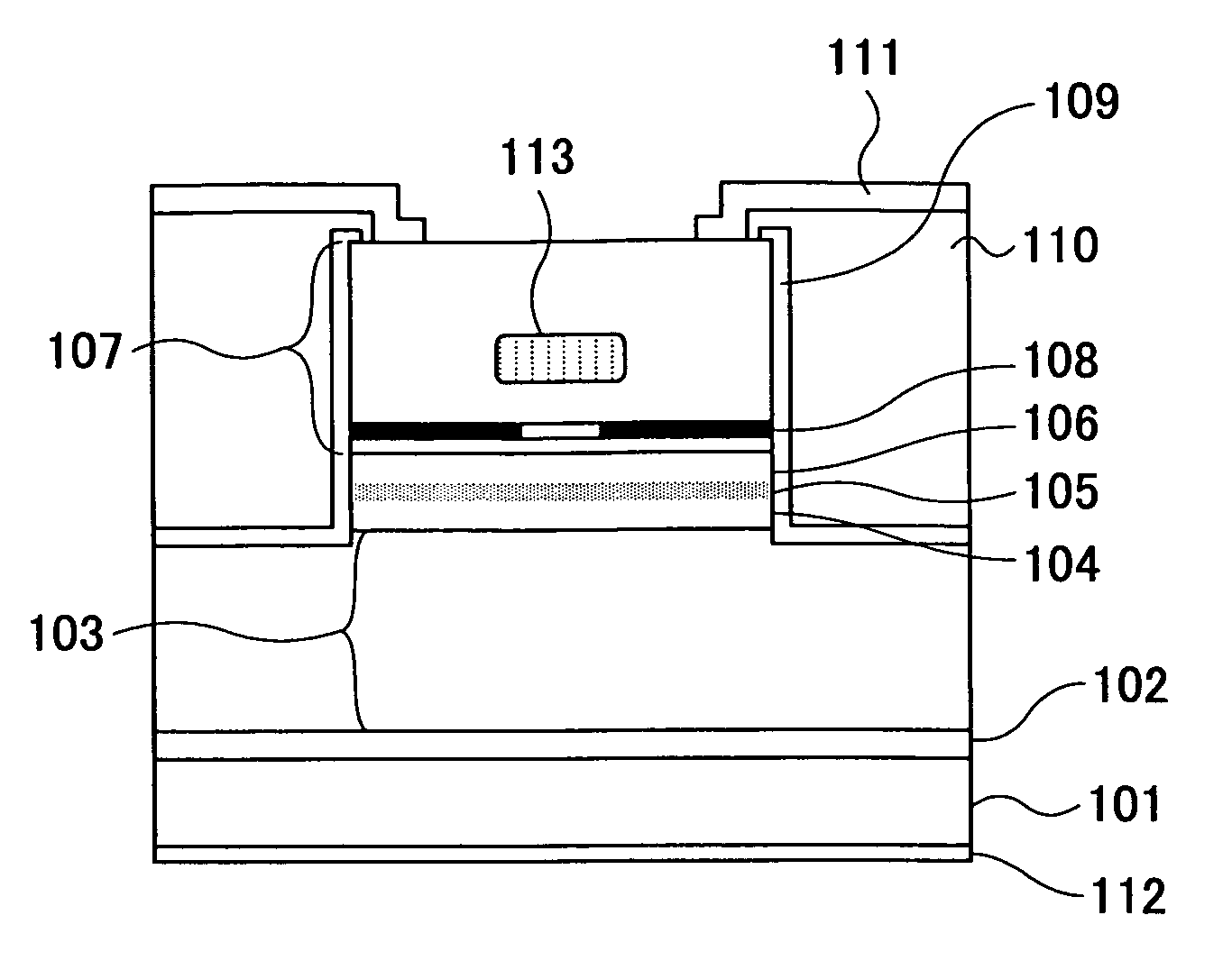
[0358]FIG. 1 shows a surface-emission laser diode according to Example 1 of the present invention, wherein the laser diode of FIG. 1 is a surface-emission laser diode having an active layer formed of a multiple quantum well structure of GaAs / Al0.15Ga0.85As and operating in the 0.85 μm band.

[0359]Hereinafter, the fabrication process of the surface-emission laser diode will be explained according to the fabrication process thereof.

[0360]Referring to FIG. 1, the surface-emission laser diode is based on the layered structure formed by an organic metal chemical vapor deposition (MOCVD) process, wherein the layered structure is formed by using trimethyl aluminum (TMA), trimethyl gallium (TMG) and trimethyl indium (TMI) for the source of the group III elements and by using an arsine (AsH3) gas for the group V source. Further, CBr4 is used for the p-type dopant and H2Se is used for the n-type dopant.

[0361]More specifically, the device of FIG. 1 is constructed on an n-GaAs substrate 101 and ...

example 2

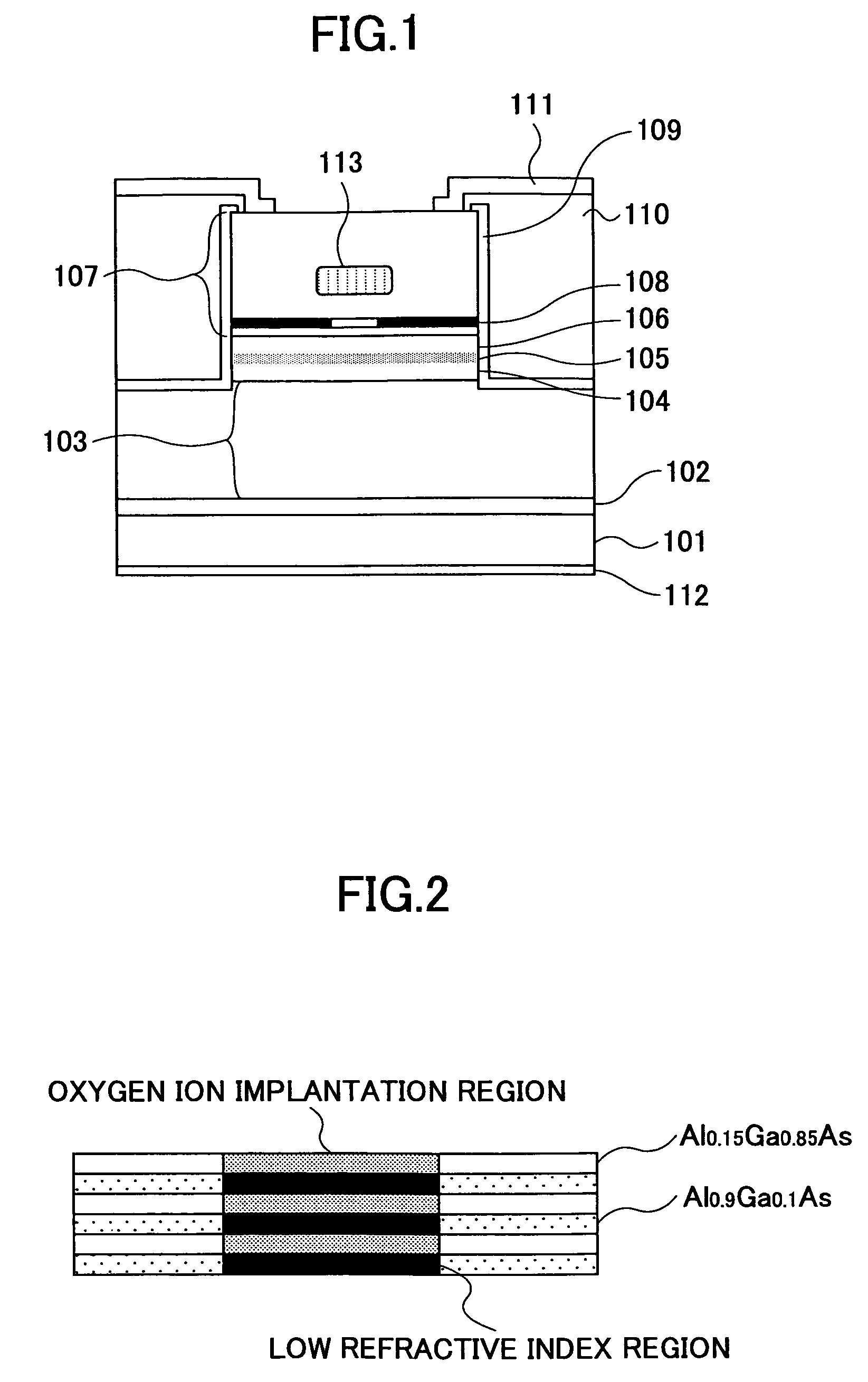
[0379]FIGS. 4 and 5 are diagrams for explaining the surface-emission laser diode according to Example 2 of the present invention.

[0380]Referring to FIG. 4, the laser diode of Example 2 is formed similarly to the laser diode of FIG. 1 up to an intermediate part of the p-type distributed Bragg reflector by a crystal growth process.

[0381]With Example 2, the crystal growth is made up to the foregoing intermediate part of the p-type distributed Bragg reflector, wherein the crystal growth is interrupted in this state and ion implantation of the molecules containing oxygen is conducted to the region that forms the central part of the mesa structure. After the ion implantation process, thermal annealing process is conducted for recovering the crystal defects caused by ion implantation, and the remaining part of the device is formed by conducting a regrowth process.

[0382]As a result of the thermal annealing process conducted for recovering the crystal defect and as a result of the heating at...

example 3

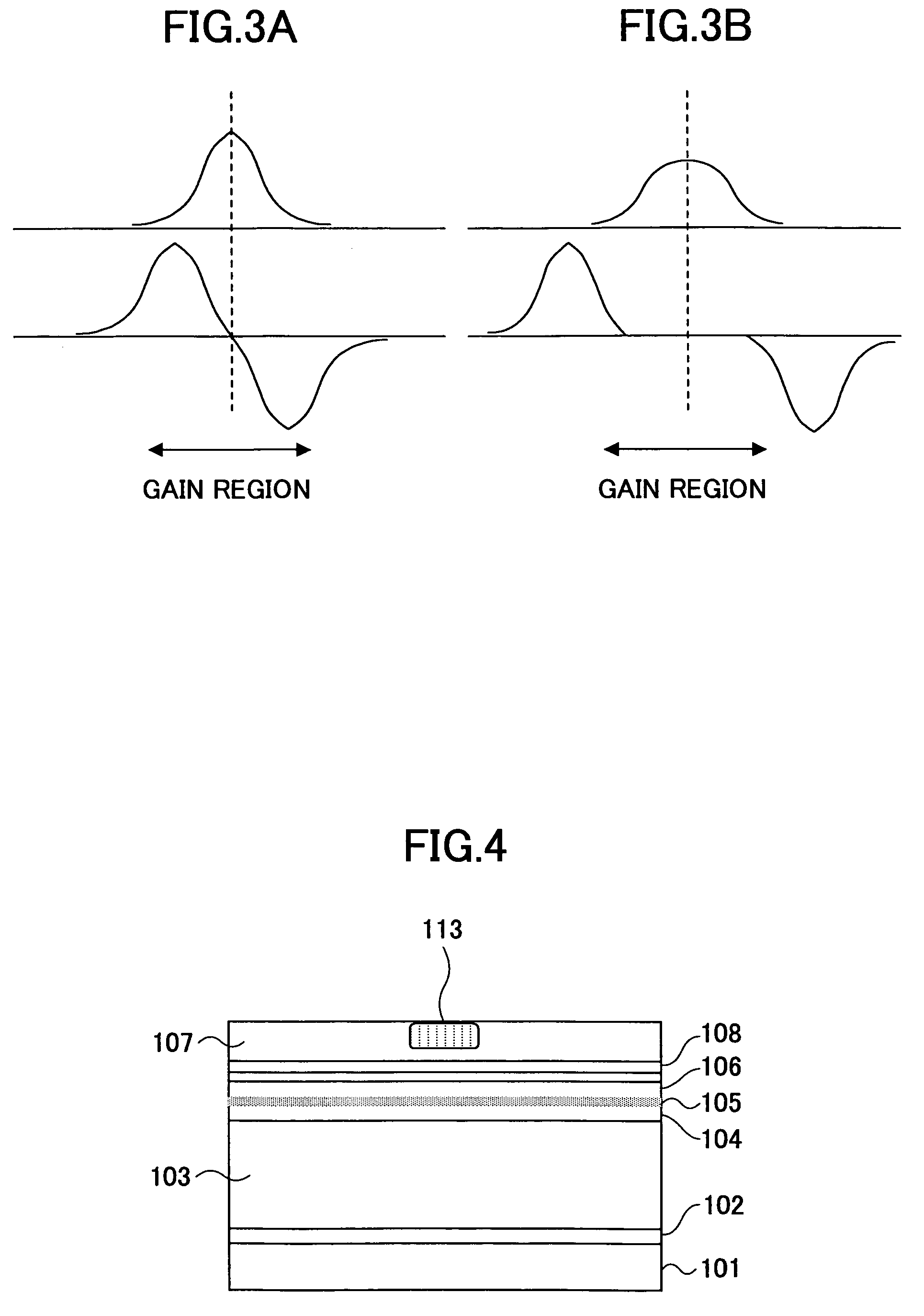
[0391]FIG. 6 explains the surface-emission laser diode of Example 3.

[0392]Referring to FIG. 6, it will be noted that the construction of the region surrounding the antiguiding structure 113 in the surface-emission laser diode of FIG. 1 is changed in the case of the device of Example 3.

[0393]In more detail, in the example of FIG. 6, the Al0.9Ga0.1As mixed crystal layer provided for forming the low refractive index layer after the selective oxidation process conducted by ion implantation of the molecules containing oxygen and subsequent thermal annealing process, is grown with increased doping concentration level as compared with the Al0.9Ga0.1As layers used for other regions. The process of device fabrication itself is identical with the case of the device of Example 1.

[0394]It should be noted that a semiconductor material doped to high concentration level shows distinctive optical absorption caused by free carrier absorption. In the case of a p-type semiconductor, in particular, the...


PUM


Abstract

A surface-emission laser diode includes an active layer, a pair of cavity spacer layers formed at both sides of the active layer, a current confinement structure defining a current injection region into the active layer, and a pair of distributed Bragg reflectors opposing with each other across a structure formed of the active layer and the cavity spacer layers, the current confinement structure being formed by a selective oxidation process of a semiconductor layer, the pair of distributed Bragg reflectors being formed of semiconductor materials, wherein there is provided a region containing an oxide of Al and having a relatively low refractive index as compared with a surrounding region in any of the semiconductor distributed Bragg reflector or the cavity spacer layer in correspondence to a part spatially overlapping with the current injection region in a laser cavity direction.

Description

BACKGROUND OF THE INVENTION[0001]The present invention relates to surface-emission laser diodes and surface-emission laser arrays, optical interconnection systems, optical communication systems, electro-photographic systems, and optical disk systems.[0002]In recent years, intensive studies are made with regard to surface-emission laser devices (surface-emission laser diodes) that produce a laser beam in the direction perpendicular to the substrate surface. As compared with an edge-emission laser diode, a surface-emission laser diode has a characteristically a small active layer volume, and hence, low threshold current for laser oscillation. Further, a surface-emission laser diode has an advantageous feature of the cavity structure suitable for high-speed modulation and can produce high-quality laser beam having a circular beam cross-section. Thus, a surface-emission laser diode attracts much attention in relation to the optical source of high-speed communication systems such as LAN ...

Claims


Application Information

Patent Timeline
Patent Type & Authority Patents(United States)
IPC IPC(8): H01S5/00H01S5/183H01S5/20H01S5/42
CPCH01S5/18355H01S5/423H01S5/0655H01S5/18308H01S5/18311H01S5/18319H01S5/18333H01S5/1835H01S5/18358H01S5/205H01S5/2063H01S2301/166
Inventor JIKUTANI, NAOTO
Owner RICOH KK
Why Eureka
Try Eureka