
Bit inversion in memory devices

a memory device and inversion technology, applied in the field of data transfer in memory devices, can solve the problems of significant increase in the programming time of flash memories, adverse effects on the performance speed of flash memories, and limited internal vpp supply generators or charge pumps

Inactive Publication Date: 2009-06-16
MICRON TECH INC
View PDF16 Cites 21 Cited by
  • Summary
  • Abstract
  • Description
  • Claims
  • Application Information

AI Technical Summary

Benefits of technology

The present invention provides methods, systems, and apparatus for inverting data during transfers within memory devices. The technical effects of the invention include reducing data transfer errors, improving data transfer speed, and increasing data transfer reliability. The invention can be implemented using existing memory devices and can be used in various applications such as data transfer between computer devices and flash memory devices.

Problems solved by technology

This is particularly important in flash memory devices, where the performance speed of the flash memory is adversely affected by the availability of an adequate power supply during write operations.
In addition, internal Vpp supply generators or charge pumps are limited, primarily due to economic reasons, in the amount of current which can be provided during write operations.
This segmented programming operation significantly increases the programming time of flash memories.
Accordingly, the process requires excess current to perform the second pass and it further creates unnecessary latency during the data transfer.
Correspondingly, memory devices which do not buffer the data during a data transfer consume greater amounts of power.
At the same time, these devices are performing more complex operations and demanding less power.

Method used


Image

  • Bit inversion in memory devices
  • Bit inversion in memory devices
  • Bit inversion in memory devices

Examples


Embodiment Construction

[0031]In the following detailed description of the invention, reference is made to the accompanying drawings which form a part hereof, and in which is shown, by way of illustration, specific embodiments in which the invention can be practiced. In the drawings, like numerals describe substantially similar components throughout the several views. These embodiments are described in sufficient detail to enable those skilled in the art to practice the invention. Other embodiments may be utilized and structural, logical, and electrical changes may be made without departing from the scope of the present invention. The following detailed description is, therefore, not to be taken in a limiting sense, and the scope of the present invention is defined only by the appended claims, along with the full scope of equivalents to which such claims are entitled.

[0032]The term “data stream” as used in this application is intended to be any data packet whether fixed or variable. At its lowest level the...


PUM


Abstract

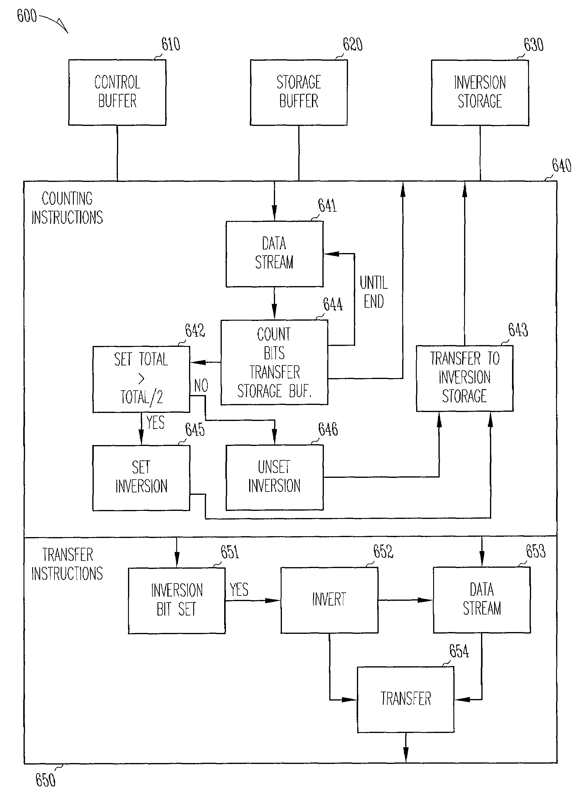
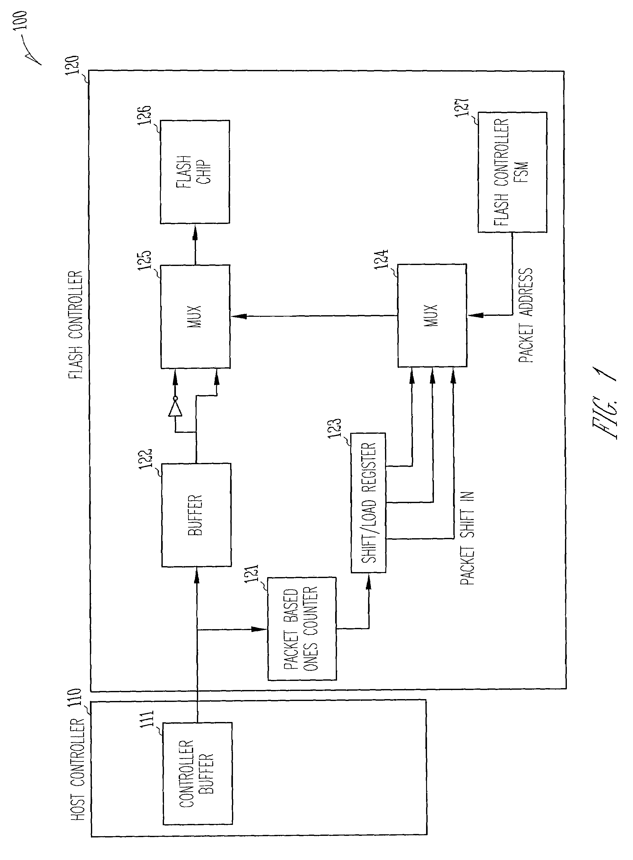
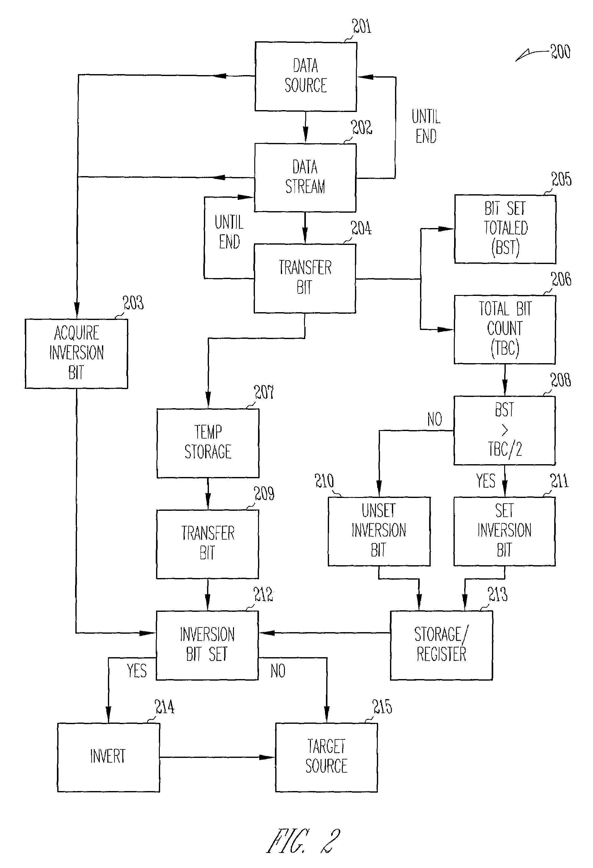
Bit inversions occurring in memory systems and apparatus are provided. Data is acquired from a source destined for a target. As the data is acquired from the source, the set bits associated with data are tabulated. If the total number of set bits exceeds more than half of the total bits, then an inversion flag is set. When the data is transferred to the target, the bits are inverted during the transfer if the inversion flag is set.

Description

TECHNICAL FIELD OF THE INVENTION[0001]The present invention relates generally to data transfers in memory devices, and in particular, the present invention relates to bit inversions on data transfers occurring between memory devices.BACKGROUND OF THE INVENTION[0002]In a memory device it is desirable to read and write data in the fastest manner possible while using the least amount of current or power as possible. As such, multiple bytes of data are often written to or read from one memory device to another memory device during a single operation. For example, during a write operation the data bits which are charged can draw current from the memory device while the data is stored. Thus, the more bits associated with the data that are set (e.g., charged having a value of “1”), the more power expended by the memory device during the write operation. However, it will be readily appreciated by those skilled in the art that some technology, which permits the programming of bits which are ...

Claims


Application Information

Patent Timeline
Patent Type & Authority Patents(United States)
IPC IPC(8): G06F12/00G11C16/10
CPCG06F12/0246G11C16/10
Inventor MOSCHOPOULOS, ANTHONY
Owner MICRON TECH INC
Learn More