Systems and methods for simultaneously testing semiconductor memory devices

a technology of memory devices and semiconductors, applied in the field of semiconductor memory devices, can solve the problems of increasing the difficulty of testing memory cell arrays, affecting the test results, and limiting the number of semiconductor memory devices which can be tested simultaneously

Inactive Publication Date: 2009-06-23
SAMSUNG ELECTRONICS CO LTD
View PDF18 Cites 18 Cited by
  • Summary
  • Abstract
  • Description
  • Claims
  • Application Information

AI Technical Summary

Problems solved by technology

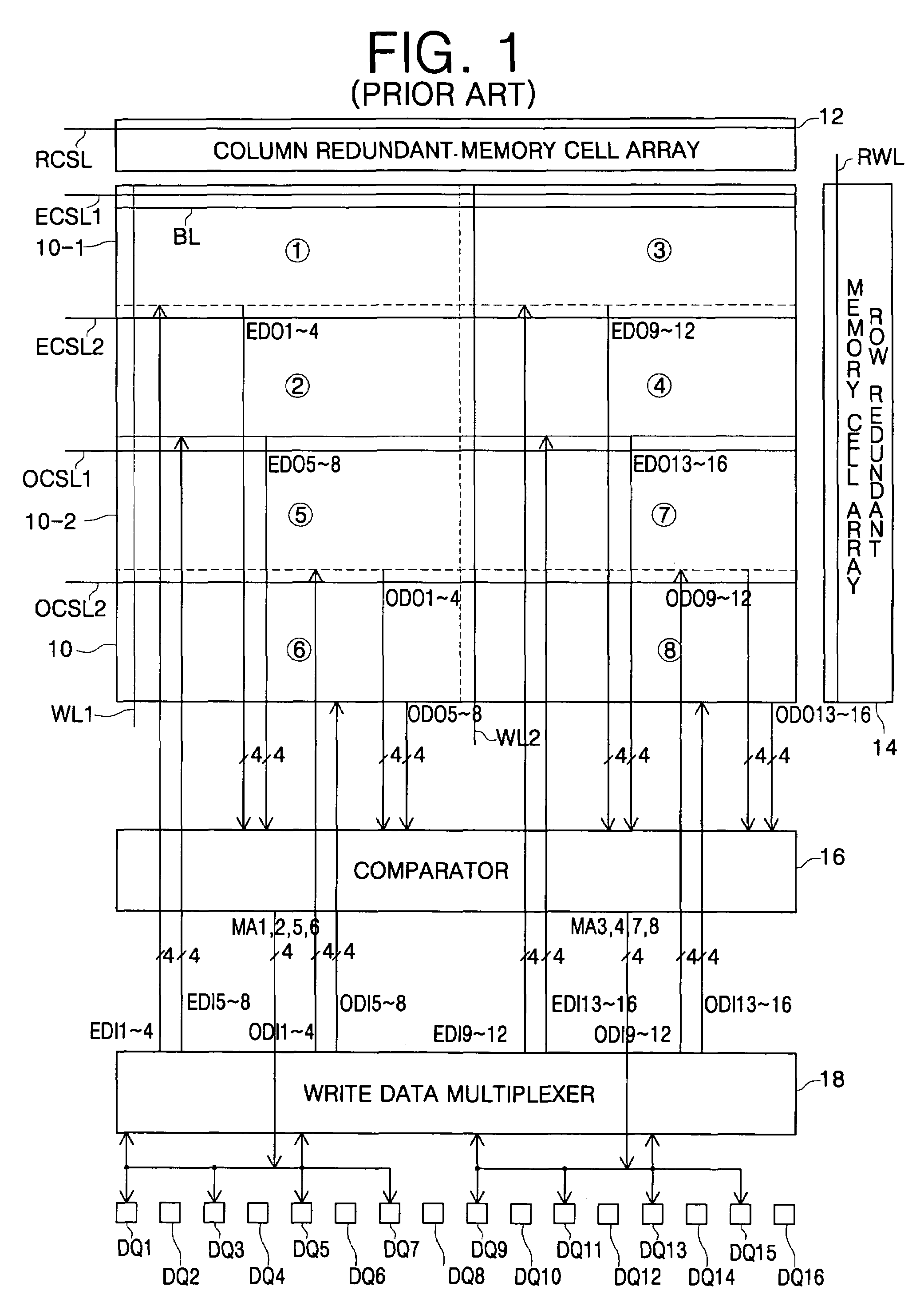
With the increased number of memory cells, it may become increasingly difficult to test the memory cell array.
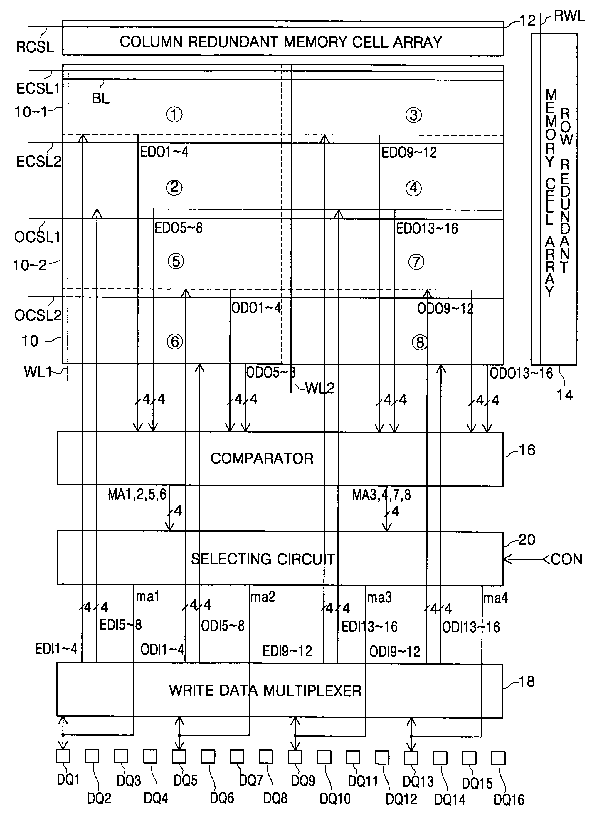
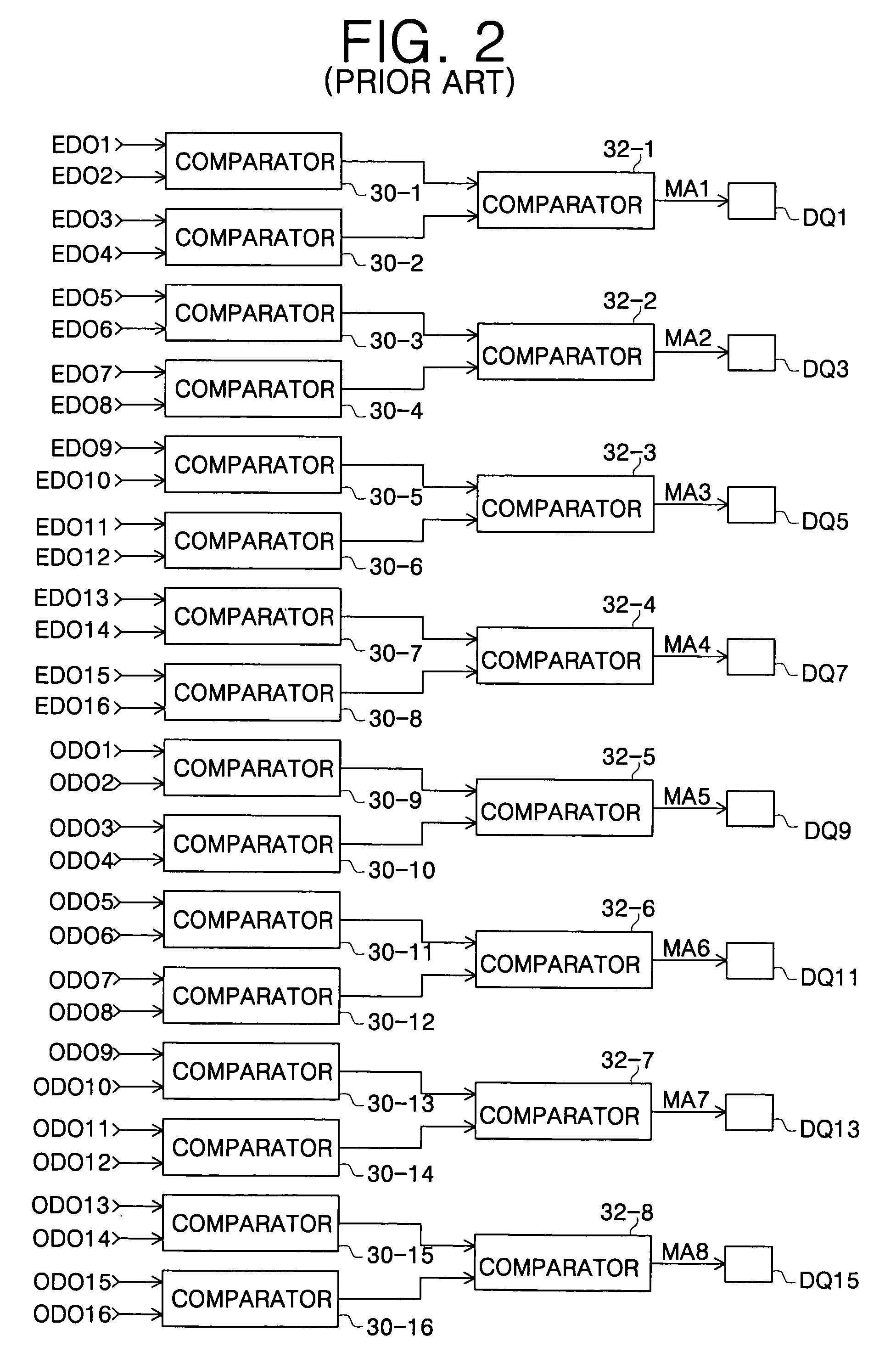
However, when the 8-bit data (MA1 to MA8) that is output from the comparators 32-1 to 32-8 is further compared by 2 bits in order to reduce the number of data I / O pads used for a read operation, the tester may not be able to correctly determine the addresses of defective memory cell locations in regions {circle around (1)} to {circle around (8)}.
As a result, the number of the semiconductor memory devices which can be tested simultaneously is limited.

Method used


Image

  • Systems and methods for simultaneously testing semiconductor memory devices
  • Systems and methods for simultaneously testing semiconductor memory devices
  • Systems and methods for simultaneously testing semiconductor memory devices

Examples


Embodiment Construction

[0027]The present invention will now be described more fully with reference to the accompanying drawings, in which preferred embodiments of the invention are shown. This invention may, however, be embodied in many different forms and should not be construed as being limited to the embodiments set forth herein. Rather, these embodiments are provided so that this disclosure will be thorough and complete and will fully convey the concept of the invention to those skilled in the art. Like numbers refer to like elements throughout.

[0028]The terminology used in the description of the invention herein is for the purpose of describing particular embodiments only and is not intended to be limiting of the invention. As used in the description of the invention and the appended claims, the singular forms “a”, “an” and “the” are intended to include the plural forms as well, unless the context clearly indicates otherwise.

[0029]It will be further understood that the terms “comprises” and / or “compr...


PUM


Abstract

A method for testing a memory cell array of a semiconductor memory device in a parallel bit test mode includes selecting first data from one of a plurality of memory regions in the memory array for output from the memory device via an input / output pad, and then selecting second data from another of the plurality of memory regions for output via the input / output pad. The first and second data can be selected from memory regions sharing a row select or a column select control line. Alternatively, one of the first and second data can be selected from memory regions sharing a row select control line, and the other can be selected from memory regions sharing a column select control line. Therefore, a parallel bit test can be performed using fewer input / output pads, and a larger number of semiconductor memory devices can simultaneously be tested. Related circuits are also discussed.

Description

RELATED APPLICATION[0001]This U.S. nonprovisional patent application claims priority under 35 U.S.C. § 119 from Korean Patent Application No. 2003-38890 filed Jun. 16, 2003, the entire contents of which is hereby incorporated by reference.BACKGROUND OF THE INVENTION[0002]1. Field of the Invention[0003]The present invention relates to semiconductor memory devices, and more particularly to systems and methods for testing semiconductor memory devices.[0004]2. Description of Related Art[0005]Integrated circuit memory devices are widely used in consumer and commercial electronics. As the integration density of these devices continues to increase, the number of cells in a memory cell array may continue to increase. With the increased number of memory cells, it may become increasingly difficult to test the memory cell array.[0006]As is well known to those of skill in the art, a memory cell array generally includes a plurality of data line outputs. In a normal, non-test mode, the data on th...

Claims


Application Information

Patent Timeline
Patent Type & Authority Patents(United States)
IPC IPC(8): G11C29/00G11C29/48
CPCG11C29/1201G11C29/48G11C2029/2602G11C29/00
Inventor KIM, JOUNG-YEALKIM, KYOUNG-HO
Owner SAMSUNG ELECTRONICS CO LTD
Why Eureka
Try Eureka