Nanotube-on-gate FET structures and applications

a technology of nanotubes and transistors, applied in the field of nonvolatile transistor structures, can solve the problems of long write cycles (ms), low relative speed in comparison to dram or sram, and relatively low cost of rom,

Inactive Publication Date: 2007-11-13
NANTERO +1
View PDF133 Cites 125 Cited by
  • Summary
  • Abstract
  • Description
  • Claims
  • Application Information

AI Technical Summary

Problems solved by technology

ROM is relatively low cost but cannot be rewritten.
EEPROM (or “Flash”) is inexpensive, and has low power consumption but has long write cycles (ms) and low relative speed in comparison to DRAM or SRAM.
Flash also has a finite number of read / write cycles leading to low long-term reliability.
SRAM does not need to be refreshed and is fast relative to DRAM, but has lower density and is more expensive relative to DRAM.
Both SRAM and DRAM are volatile, meaning that if power to the memory is interrupted the memory will lose the information stored in the memory cells.
Consequently, existing technologies are either non-volatile but are not randomly accessible and have low density, high cost, and limited ability to allow multiples writes with high reliability of the circuit's function, or they are volatile and complicate system design or have low density.
A different memory cell based upon magnetic tunnel junctions has also been examined but has not led to large-scale commercialized MRAM devices.
FRAM suffers from a large memory cell size, and it is difficult to manufacture as a large-scale integrated component.
While the nonvolatility condition is met, this technology appears to suffer from slow operations, difficulty of manufacture and reliability and has not reached a state of commercialization.
This form of memory requires highly specialized wire junctions and may not retain non-volatility owing to the inherent instability found in redox processes.
These techniques are now believed to be difficult to employ at commercial scales using modern technology.
Moreover, they may contain inherent limitations such as the length of the nanotubes that may be grown reliably using these techniques, and it may difficult to control the statistical variance of geometries of nanotube wires so grown.

Method used


Image

  • Nanotube-on-gate FET structures and applications
  • Nanotube-on-gate FET structures and applications
  • Nanotube-on-gate FET structures and applications

Examples


Embodiment Construction

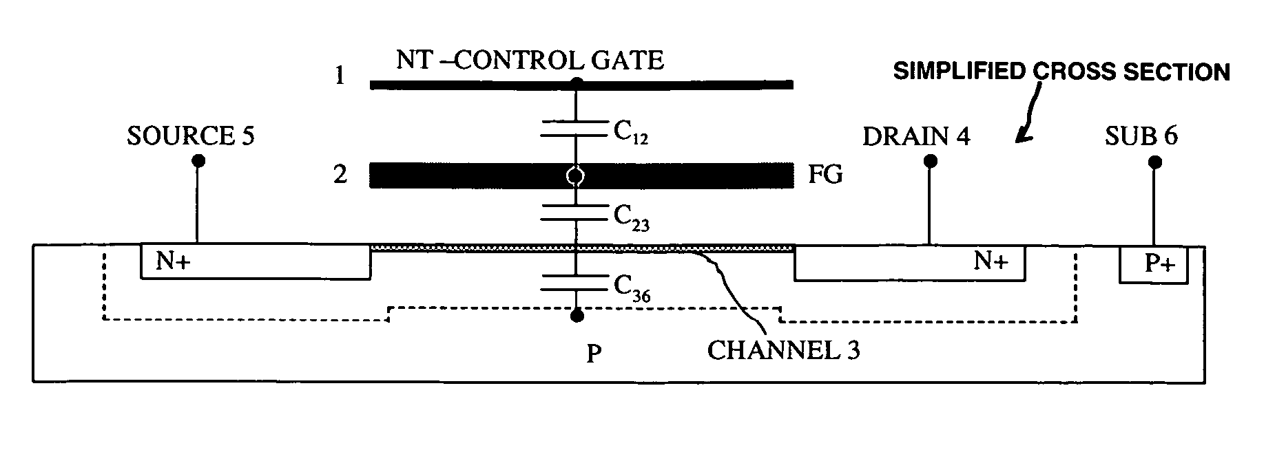
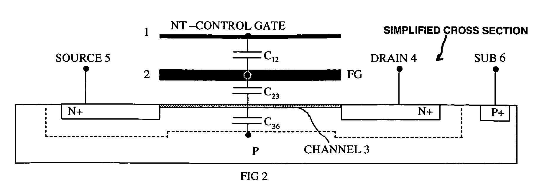
[0067]The NT electromechanical switching components in the described embodiments incorporate a nanofabric component. More specifically, preferred embodiments provide transistor devices in which a nanotube switching element is integrated into a control element of the transistor, such as the gate of a FET device. (Nanotube switching elements are described in more detail in other applications and / or patents identified below, and are discussed herein to the extent relevant for understanding the preferred embodiments.)

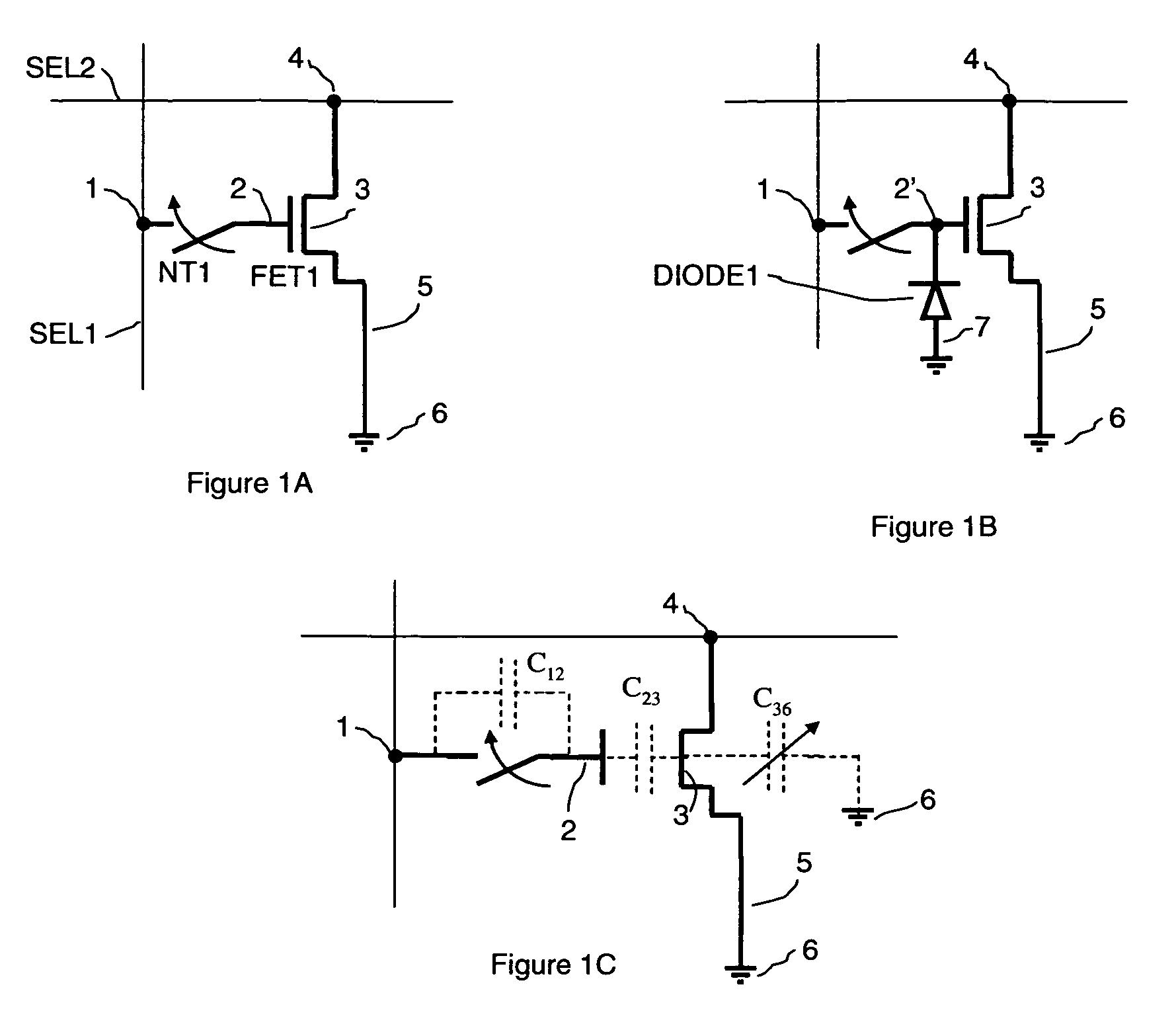
[0068]FIG. 1A illustrates a nanotube (NT)-on-gate of FET approach. This structure utilizes a nanofabric-based switch NT1 which controls the FET transistor gate which controls the transistor channel, and therefore the current through the transistor as shown. The gate voltage of FET1 is not defined; it floats. Therefore if a voltage is applied to node 1 using SEL1, the voltage across nanotube NT1 is not known.

[0069]FIG. 1B changes the arrangement by adding DIODE1 between subs...


PUM


Abstract

Nanotube on gate FET structures and applications of such, including n2 crossbars requiring only 2n control lines. A non-volatile transistor device includes a source region and a drain region of a first semiconductor type of material and a channel region of a second semiconductor type of material disposed between the source and drain region. A gate structure is made of at least one of semiconductive or conductive material and is disposed over an insulator over the channel region. A control gate is made of at least one of semiconductive or conductive material. An electromechanically-deflectable nanotube switching element is in fixed contact with one of the gate structure and the control gate structure and is not in fixed contact with the other of the gate structure and the control gate structure. The device has a network of inherent capacitances, including an inherent capacitance of an undeflected nanotube switching element in relation to the gate structure. The network is such that the nanotube switching element is deflectable into contact with the other of the gate structure and the control gate structure in response to signals being applied to the control gate and one of the source region and drain region. Certain embodiments of the device have an area of about 4 F2. Other embodiments include a release line is positioned in spaced relation to the nanotube switching element, and having a horizontal orientation that is parallel to the orientation of the source and drain diffusions. Other embodiments provide an n2 crossbar array having n2 non-volatile transistor devices, but require only 2n control lines.

Description

CROSS-REFERENCE TO RELATED APPLICATIONS[0001]This application claims priority under 35 U.S.C. § 119(e) to U.S. Provisional Pat. Apl. Ser. No. 60 / 459,224, filed on Mar. 28, 2003, entitled Nanotube-On-Gate FET Structures and Applications, which is incorporated herein by reference in its entirety.[0002]This application is related to the following U.S. applications, the contents of which are incorporated herein in their entirety by reference:[0003]U.S. Provisional Apl. Ser. No. 60 / 459,223 filed on Mar. 28, 2003, entitled NRAM Bit Selectable Two-Device Nanotube Array; and U.S. patent application Ser. No. 10 / 810,962, filed on the same day as the present application, entitled NRAM Bit Selectable Two-Device Nanotube Array.[0004]U.S. Provisional Patent Application No. 60 / 459,253, filed on Mar. 28, 2003, entitled Single Transistor with Integrated Nanotube (NT-FET), and U.S. patent application Ser. No. 10 / 459,253, filed on the same day as the present application, entitled A Four Terminal Non-V...

Claims


Application Information

Patent Timeline
Patent Type & Authority Patents(United States)
IPC IPC(8): H01L51/30G11C13/02G11C16/04G11C23/00H01L27/108H01L29/06H01L29/423H01L29/76H01L29/94H01L31/119H01L51/00
CPCB82Y10/00G11C13/025G11C23/00H01L51/055H01L29/0673H01L29/42324H01L29/0665G11C16/0416G11C2213/17H01L51/0048H01L51/0052H10K85/221H10K85/615H10K10/481
Inventor RUECKES, THOMASSEGAL, BRENT M.VOGELI, BERNARDBROCK, DARREN K.JAIPRAKASH, VENKATACHALAM C.BERTIN, CLAUDE L.
Owner NANTERO
Why Eureka
Try Eureka