Memory device with a selection element and a control line in a substantially similar layer

a memory device and control line technology, applied in semiconductor devices, diodes, electrical devices, etc., can solve the problems of sensitivity to alignment tolerances, more complex devices require more individual layers to implement, and generally do not retain information stored or programmed within, so as to reduce the complexity of vertical stacking, and mitigate the effect of vertical stacking

Active Publication Date: 2008-06-24
MONTEREY RES LLC
View PDF1 Cites 109 Cited by
  • Summary
  • Abstract
  • Description
  • Claims
  • Application Information

AI Technical Summary

Benefits of technology

[0007]The subject invention provides semiconductor memory devices and methods for forming such devices, wherein a selection element of a device is formed in a substantially similar layer as one or more control lines (e.g. wordlines and bitlines). In accordance with one aspect of the invention, producing such memory device requires fewer layers to implement than conventional techniques, thereby reducing complexity of vertical stacking. In addition, formation of the selection element within the substantially similar layer as a wordline or bitline can mitigate vertical stacking issues, increase device yield and reduce related production costs. It is to be appreciated that in one instance a diode can be utilized as the selection element.
[0008]The invention also facilitates manufacture of densely populated semiconductor memory components through reducing the number of layers required to implement semiconductor memory devices within memory components. In such components, control voltages can be applied to wordlines and / or bitlines to facilitate writing, erasing, and / or reading a single memory device within an array of semiconductor memory devices. The unique characteristics of diodes allow them to function as selection elements and facilitate application of control voltages to accomplish such writing, erasing, and / or reading. In this manner, each memory device within an array of memory devices can be programmed with similar or disparate data or states.

Problems solved by technology

Volatile memory components generally do not retain information stored or programmed within them when power is removed from the component.
In general, more complex devices require more individual layers to implement.
With the size of semiconductor features decreasing and number of layers increasing, sensitivity to alignment tolerances makes fabrication markedly more difficult.
As the number of layers required to produce a semiconductor device increases, manufacturing defects generally increase and, therefore, the yield decreases.

Method used


Image

  • Memory device with a selection element and a control line in a substantially similar layer
  • Memory device with a selection element and a control line in a substantially similar layer
  • Memory device with a selection element and a control line in a substantially similar layer

Examples


Embodiment Construction

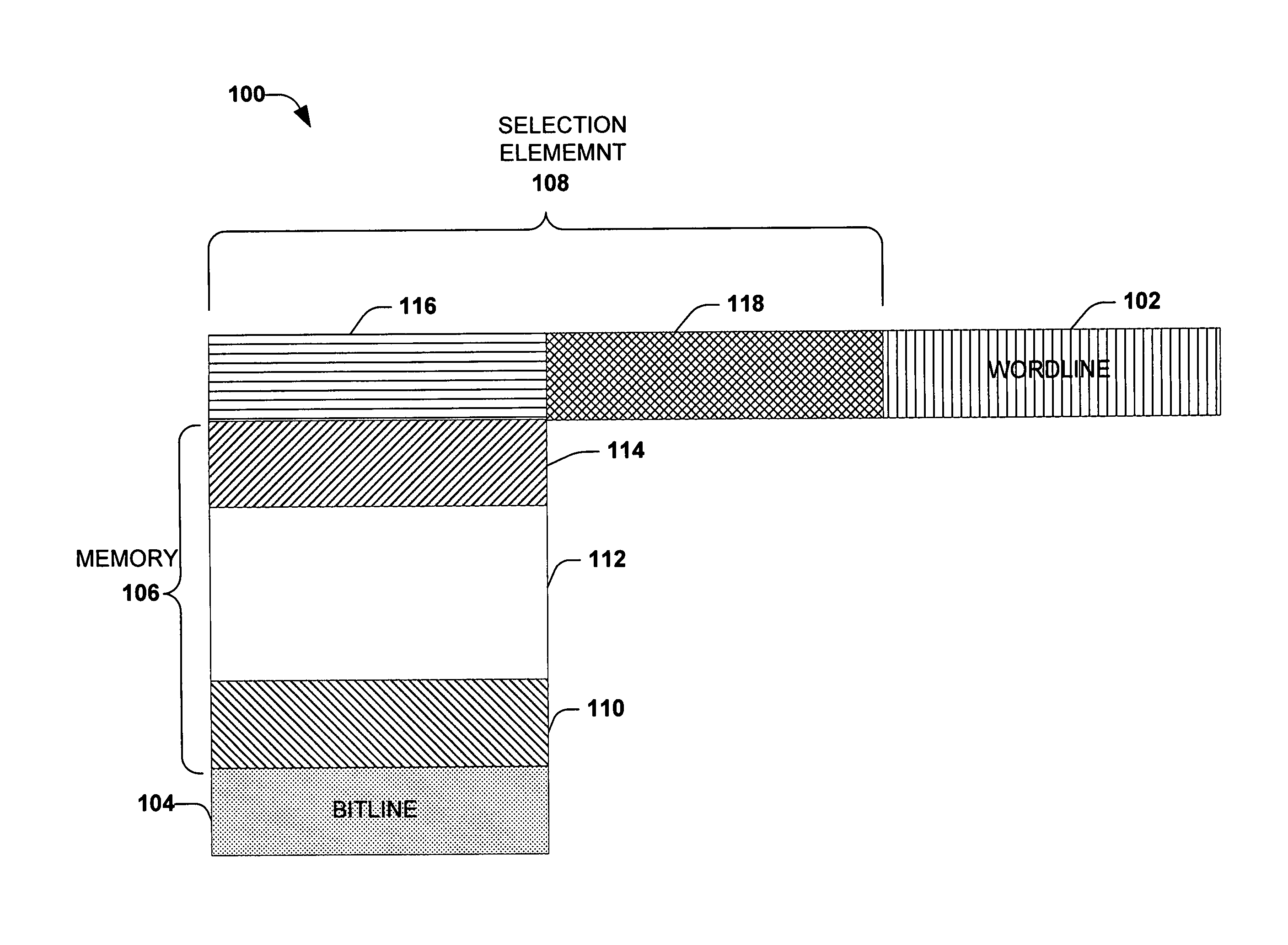
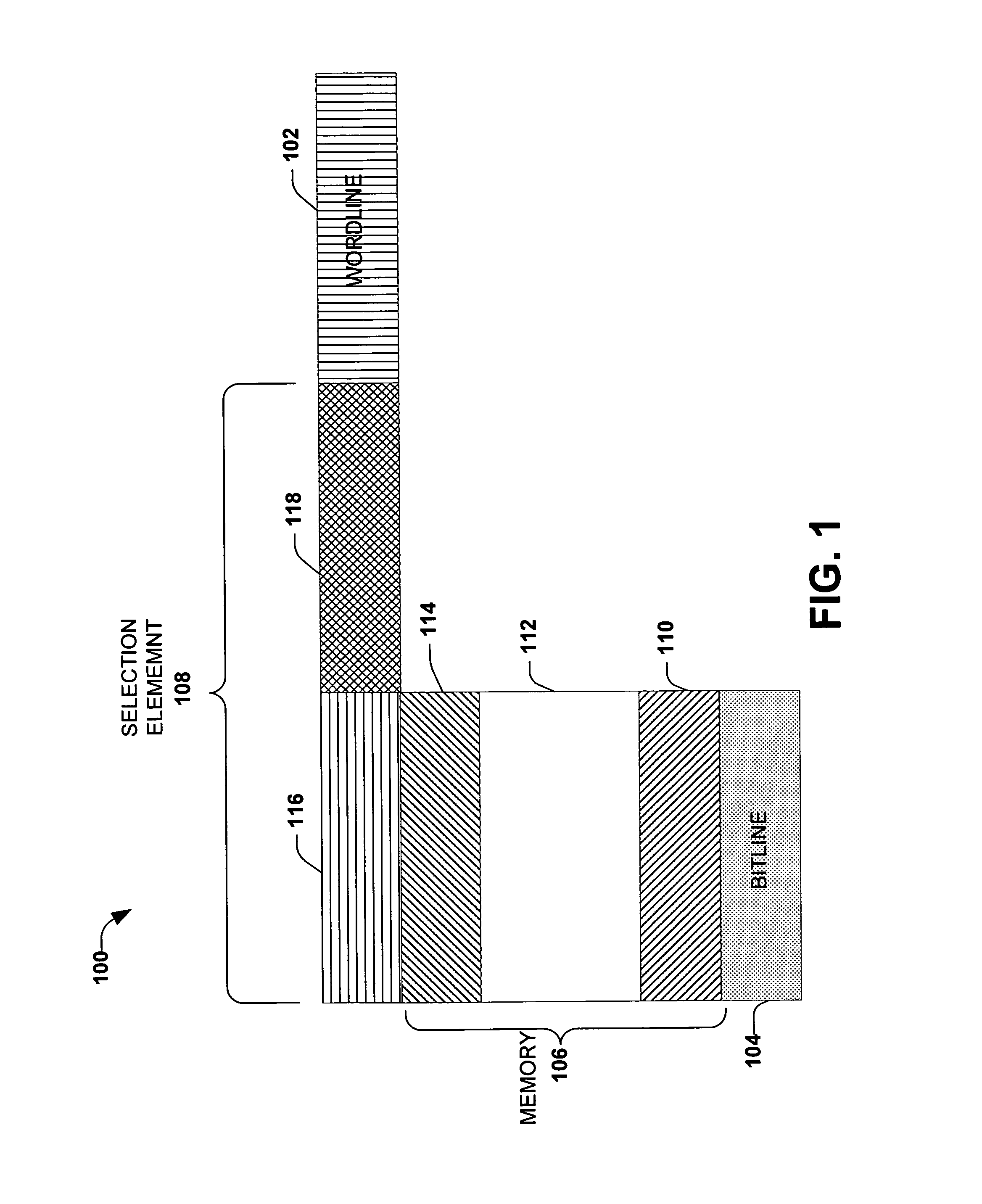
[0025]The subject invention provides a semiconductor memory device with a selection element in a substantially similar layer as a control line, which can reduce complexity associated with vertical stacking techniques utilized to implement memory devices. The invention further provides methods of making such memory devices. The selection element facilitates selection of a specific memory element to be written, read, or erased. Traditional memory devices generally form the selection element through the deposition of separate layers within a semiconductor chip, and many conventional memory arrays stack memory devices, for example, one upon another, in a vertical manner, which can increase the number of memory devices stacked upon another. The subject invention reduces complexity of vertical stacking by incorporating the selection element (e.g. a diode) into the layer where one of the control lines (e.g. a wordline and a bitline) resides. In one aspect of the invention, the selection el...


PUM


Abstract

The invention facilitates manufacture of semiconductor memory components by reducing the number of layers required to implement a semiconductor memory device. The invention provides for a selection element to be formed in the same layer as one of the control lines (e.g. one of the wordline and bitline). In one embodiment of the invention, a diode is implemented as the selection element within the same layer as one of the control lines. Production of the selection element within the same layer as one of the wordline and bitline reduces problems associated with vertical stacking, increases device yield and reduces related production costs. The invention also provides an efficient method of producing memory devices with the selection element in the same layer as one of the control lines.

Description

FIELD OF INVENTION[0001]The subject invention relates generally to semiconductor devices and, in particular, to a semiconductor memory device with a selection element and a control line in a substantially similar layer of the semiconductor memory device.BACKGROUND OF THE INVENTION[0002]The reduction in size of semiconductor components and increased usage of semiconductor processors has lead to an explosion of new electronic devices. Most, if not all, of these electronic devices require some amount of memory in order to function. The proliferation of such devices has significantly increased demand for memory that is efficient in size as well as power consumption. Smaller sized semiconductor components and memories have made numerous hand held electronic devices feasible. Examples of hand-held devices include cell phones, personal radios, walkie-talkies, personal data assistants, palm pilots, pagers, notebook computers, remote controls, voice recorders, audio recorders, video recorder...

Claims


Application Information

Patent Timeline
Patent Type & Authority Patents(United States)
IPC IPC(8): H01L29/80
CPCH01L27/101H01L27/1021
Inventor TRIPSAS, NICHOLAS H.PANGRLE, SUZETTE
Owner MONTEREY RES LLC
Why Eureka
Try Eureka