Microwave photonic delay line with separate tuning of optical carrier

a microwave photonic delay and optical carrier technology, applied in optics, instruments, antennas, etc., can solve the problems of time delay, inability to easily tune, and inherently small size of photonic devices

Active Publication Date: 2009-07-07
MORTON PHOTONICS INC
View PDF1 Cites 17 Cited by
  • Summary
  • Abstract
  • Description
  • Claims
  • Application Information

AI Technical Summary

Benefits of technology

[0018]In the preferred embodiment the device comprises at least three integrated microresonators having resonance frequencies ω1=ωr−Δω1, ω2=ωr+Δω1, and ω3=ω0±Δω2 respectively, ωr is a median frequency of the side band, ω0 is the carrier frequency, and Δω1,2 are deviations from those frequencies. The third resonator provides a phase delay difference between the phase at the optical carrier frequency Φ(ω0) and the phase at the median signal frequency Φ(ωr) equal to (ω0−ωr)Td, where Td is the time delay. The frequency ω3 is chosen to satisfy the relation Φ(ω0)=Φ(ωr)+Td(ωr)(ω0−ωr). The first two resonators in the group provide tunable group delay for the signal band, while the remaining at least one resonator provides tunable phase delay for the optical carrier. The first and the second resonators eliminate a third order group delay dispersion over the side band frequencies of the signal band using cancellation of the positive dispersion of the first loop resonator by the negative dispersion of equal magnitude of the second loop resonator. This arrangement allows one to operate as a true time delay line for very high frequency but relatively narrow band RF signals.

Problems solved by technology

Photonic devices are inherently small due to the short wavelength at which they operate (around 1 micron) compared to the cm and mm wavelengths of microwave integrated circuits in phased array systems.
In the state of the art phased arrays the true time delay can be achieved only by using long propagation length, and it cannot be tuned easily.

Method used


Image

  • Microwave photonic delay line with separate tuning of optical carrier
  • Microwave photonic delay line with separate tuning of optical carrier
  • Microwave photonic delay line with separate tuning of optical carrier

Examples


Embodiment Construction

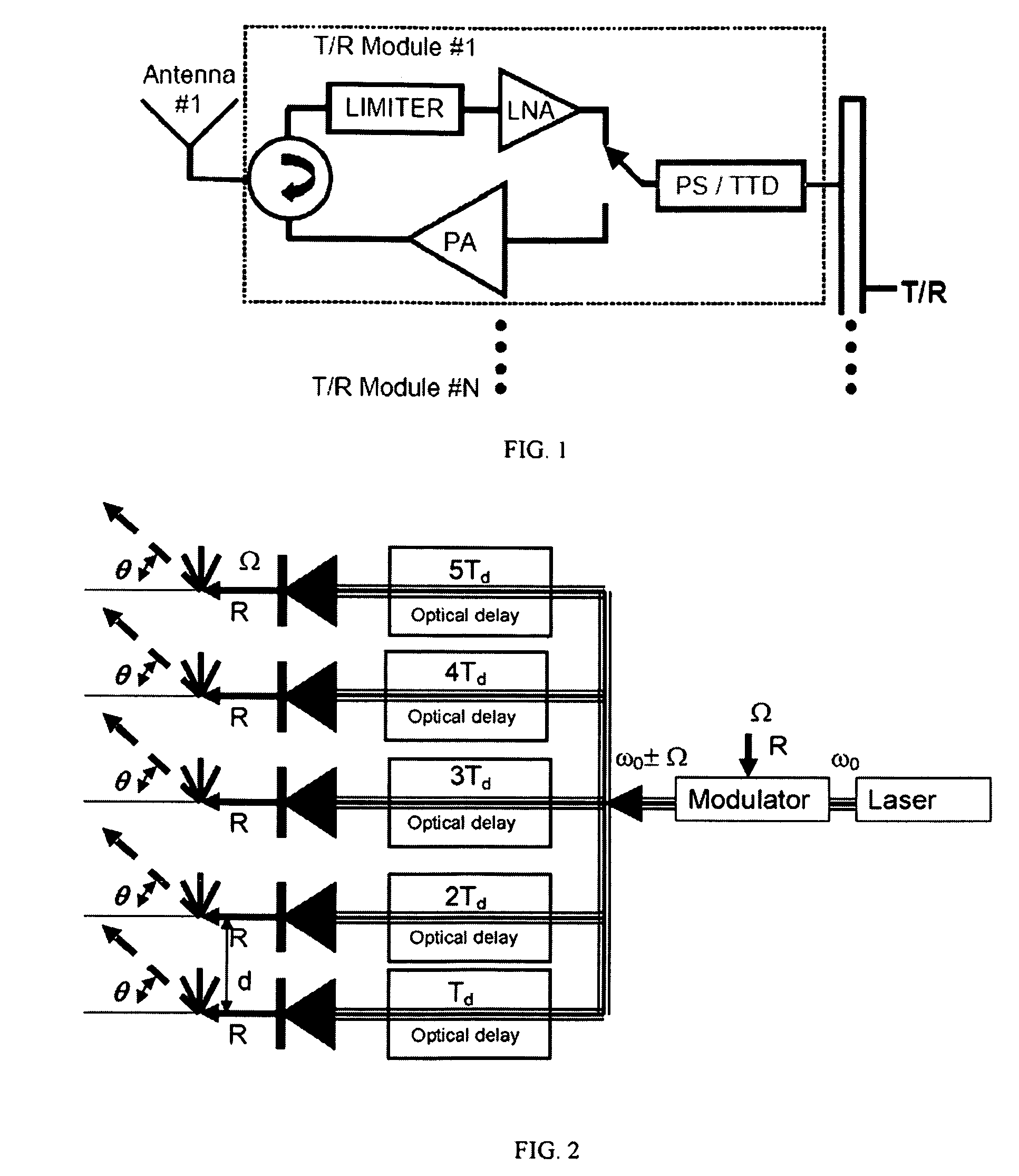
[0034]Optical delay lines typically use near infrared (NIR) light, however the disclosure is not limited to this spectral range. The term “optical” in the present disclosure comprises visible, near infrared, infrared, far infrared and the near and far ultra-violet spectra.

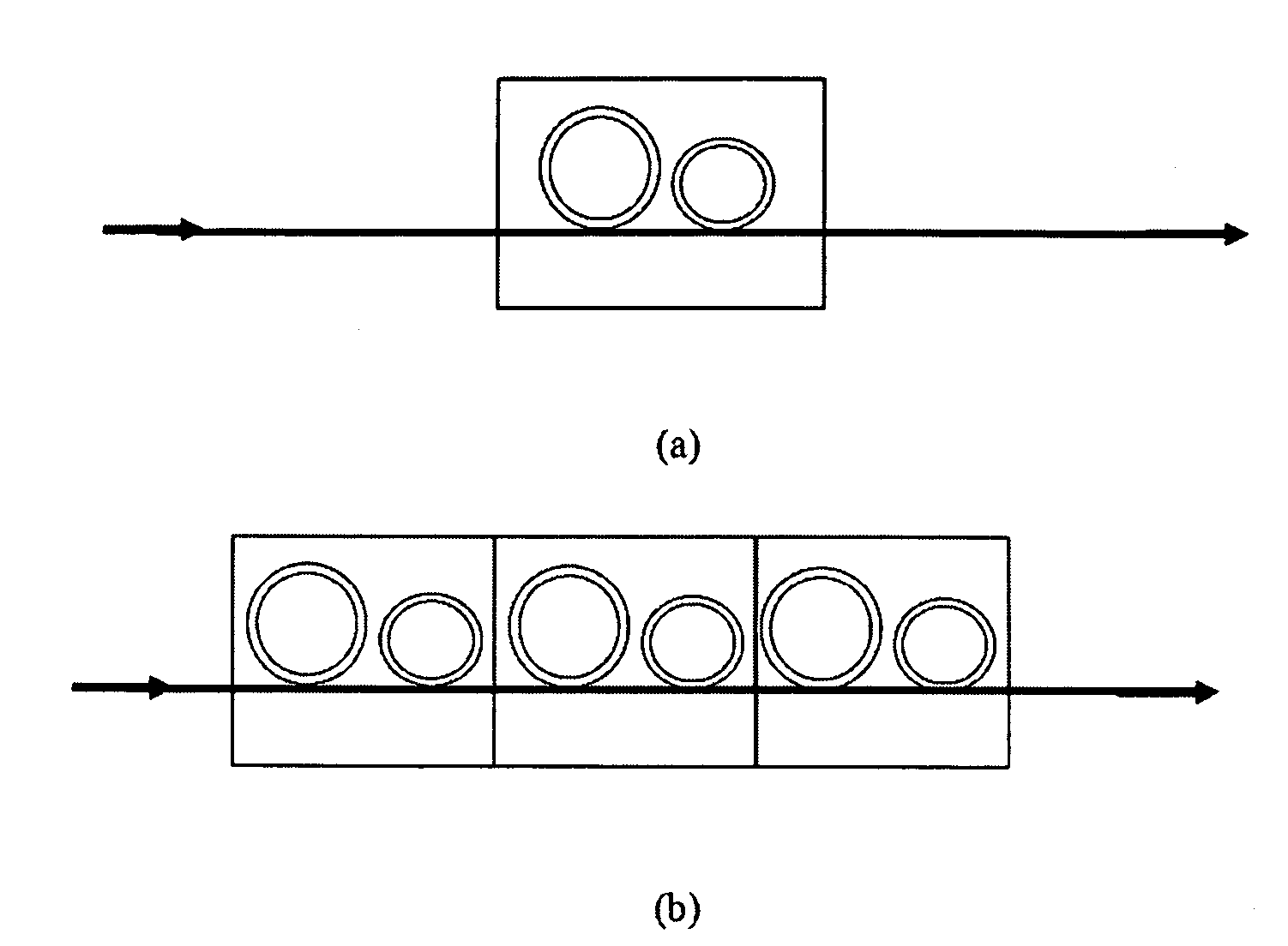
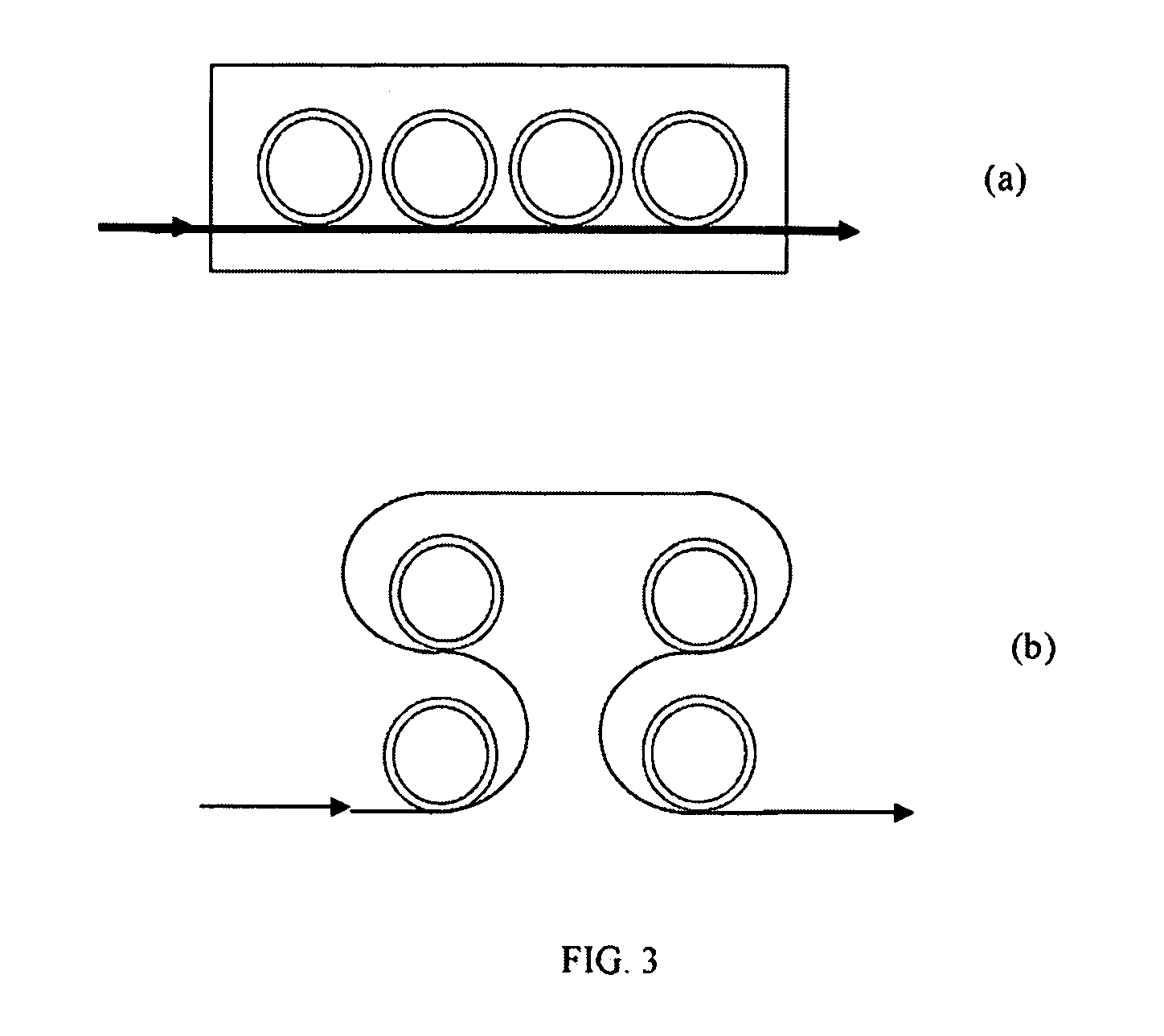
[0035]The novel approach is applied to the processing of the optical signal for use in phased array antennas based on separate processing of the optical carrier, the upper sideband, and the lower sideband of the modulated optical signal. This technology has a number of potential implementations, which utilize the ideas of separately controlling the time delay of each signal, and also removing one of the sideband signals through optical filtering. The filtering and also separate control of each signal can be most easily implemented when the modulation frequency is high, so that separation between the optical carrier and sidebands is large. A good example of this would be a 60 GHz RF frequency modulated onto an optic...


PUM

PropertyMeasurementUnit
radiusaaaaaaaaaa
wavelengthsaaaaaaaaaa
center frequencyaaaaaaaaaa

Abstract

This invention provides a tunable delay of an optical signal having a carrier with an angular frequency ω0 and a single side band having a signal band with a median angular frequency ωr. The delay line comprises at least a first, a second and a third integrated resonators coupled sequentially to a waveguide. The first and the second resonators have angular resonant frequencies ω1=ωr−Δω and ω2=ωr+Δω respectively, where Δω is a deviation from the median frequency. The third resonator provides a phase delay difference between the phase at the optical carrier ω0 and the phase at the median frequency ωr equal to (ωr−ω0)Td, where Td is the time delay. The device provides an equal group delay to all frequency components in the output signal and also equal phase delay for all frequency components of an RF signal when the optical signal is downconverted at a photodetector. The device may find applications controlling the time delay to antenna elements in a phased array system.

Description

CROSS-REFERENCE TO RELATED APPLICATIONS[0001]The application claims priority of U.S. Provisional Patent Application Ser. No. 60 / 974,502 filed Sep. 24, 2007. This application is also a Continuation-in-part of U.S. patent application Ser. No. 12 / 205,368 filed Sep. 5, 2008.STATEMENT REGARDING FEDERAL SPONSORED RESEARCH AND DEVELOPMENT[0002]This invention was made with U.S. Government support under Contract W31P4Q-07-CO150 with DARPA MTO SBIR Project, and the U.S. Government has certain rights in the invention.FIELD OF INVENTION[0003]This invention relates to tunable optical delay lines. More particularly it addresses the use of tunable delays in phased array antenna systems.BACKGROUND OF THE INVENTION[0004]A phased array is a group of radio frequency antennas in which the relative phases of the respective signals feeding the antennas are varied in such a way that the effective radiation pattern of the array is reinforced in a desired direction and suppressed in undesired directions. In...

Claims


Application Information

Patent Timeline
Patent Type & Authority Patents(United States)
IPC IPC(8): G02F1/01G02B6/26G02B6/42
CPCH01Q3/2676
Inventor KHURGIN, JACOBMORTON, PAUL A.
Owner MORTON PHOTONICS INC
Why Eureka
Try Eureka