Flash memory device

a flash memory and memory technology, applied in the field of semiconductor memory devices, to achieve the effect of reducing read errors

Active Publication Date: 2009-07-21
SK HYNIX INC
View PDF8 Cites 8 Cited by
  • Summary
  • Abstract
  • Description
  • Claims
  • Application Information

AI Technical Summary

Benefits of technology

[0016]An embodiment of the present invention relates to a flash memory device that can reduce read errors caused by leakage current.

Problems solved by technology

In other words, a problem occurs because the selected cell can be read as an erased cell due to the leakage current although the selected cell is a programmed cell.

Method used


Image

  • Flash memory device
  • Flash memory device
  • Flash memory device

Examples


first embodiment

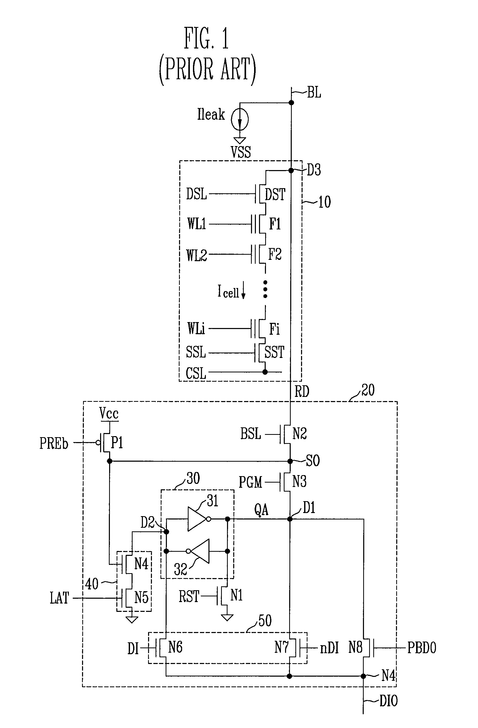
[0033]Referring to FIG. 4, according to the present invention a flash memory device 100 includes a normal memory cell array 101, a reference memory cell block 102, a plurality of normal page buffers PB1 to PBn (where n is an integer), a reference page buffer RPB, and a latch signal generator 103.

[0034]The normal memory cell array 101 includes normal memory cells for storing data. One or more reference memory cell blocks 102 store reference data. The plurality of normal page buffers PB1 to PBn serve to input data to the normal memory cell array 101 or read data stored in the normal memory cell array 101. One or more reference page buffers RPB serve to input reference data to the reference memory cell block 102 or read reference data from the reference memory cell block 102 and output a reference control signal RQA. One or more latch signal generators 130 generate first and second latch control signals LATb, LAT, which will be provided to the plurality of normal page buffers PB1 to PB...

second embodiment

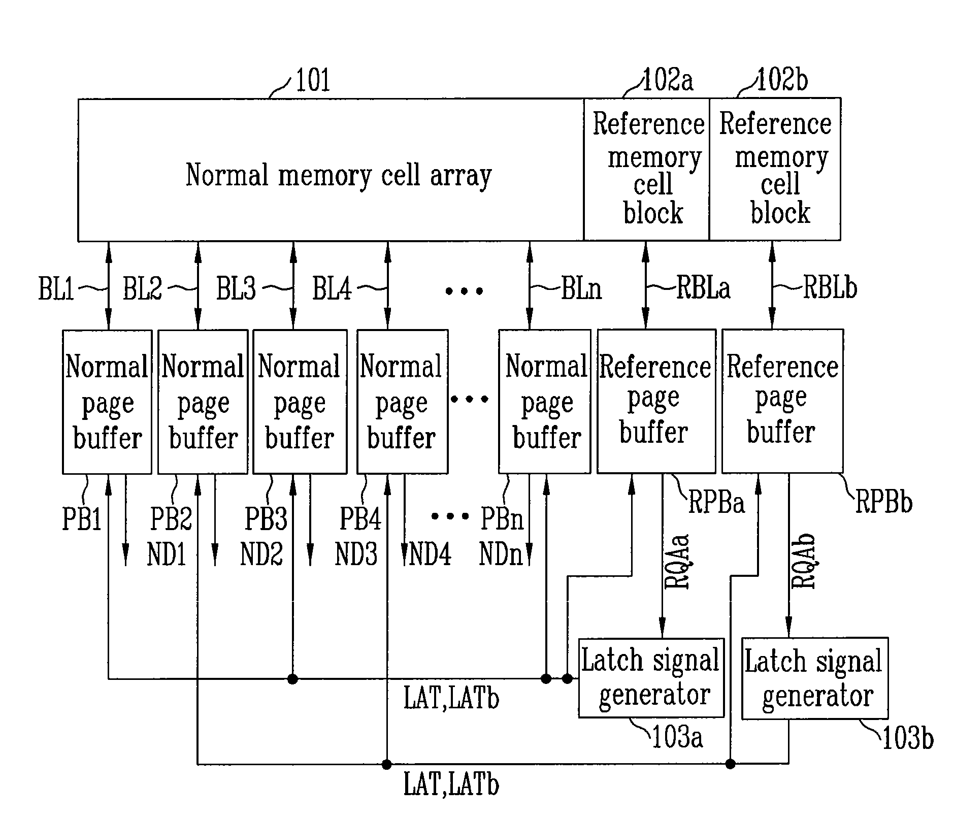
[0077]Referring to FIG. 12, according to the present invention, a flash memory device 100 includes a normal memory cell array 101, a plurality of reference memory cell blocks 102a, 102b, a plurality of normal page buffers PB1 to PBn, a plurality of reference page buffers RPBa, RPBb, and a plurality of latch signal generators 103a, 103b.

[0078]The normal memory cell array 101 is connected to the plurality of normal page buffers PB1 to PBn through bit lines BL1 to BLn. The normal memory cell array 101 outputs read data or receives program data at the time of a read or program operation. Each of the normal page buffers PB1 to PBn outputs program data to the normal memory cell array 101 at the time of a program operation and receives read data from the normal memory cell array 101 at the time of a read operation.

[0079]Each of the reference memory cell blocks 102a, 102b includes a plurality of reference memory cell strings. Each of the plurality of reference memory cell strings includes ...


PUM


Abstract

A flash memory device includes a normal memory cell array for storing data, a normal page buffer for inputting data to the normal memory cell array or reading data stored in the normal memory cell array, one or more reference memory cell blocks for storing reference data, one or more reference page buffers for inputting reference data to the reference memory cell blocks or reading reference data from the reference memory cell blocks, and outputting a reference control signal, and one or more latch signal generators for generating first and second latch control signals supplied to the normal page buffer and the reference page buffers in response to the reference control signal. A reference bit line signal is formed using the reference memory cell block, the reference page buffer, and the latch signal generator.

Description

BACKGROUND[0001]The present invention relates to semiconductor memory devices, and more particularly, to flash memory devices that reduce read errors due to leakage current.[0002]In general, semiconductor memory devices are classified into volatile or non-volatile memory devices depending on whether data is retained when the power is turned off. The non-volatile memory device is a memory device that can retain data even after the supply of power is stopped. In recent years, the flash memory device has been in the spotlight. Flash memory can be classified into a NOR or a NAND type memory device. The NAND flash memory device employs read and program methods on a page basis.[0003]The flash memory device includes a memory cell array having a plurality of memory cell strings. The plurality of memory cell strings are connected to a plurality of page buffers through bit lines.[0004]FIG. 1 is a circuit diagram of a conventional flash memory device. Referring to FIG. 1, a memory cell string ...

Claims


Application Information

Patent Timeline
Patent Type & Authority Patents(United States)
IPC IPC(8): G11C7/10
CPCG11C7/02G11C16/28G11C7/14G11C7/1021G11C16/10G11C16/24G11C2216/14
Inventor PARK, JIN SU
Owner SK HYNIX INC
Why Eureka
Try Eureka