Monolithic ceramic electronic component

a technology of electronic components and monolithic ceramics, applied in the direction of fixed capacitor details, stacked capacitors, fixed capacitors, etc., can solve the problems of cracks, structural defects, and ceramic laminates that may occur in firing steps, and achieve the effect of preventing structural defects caused by internal stress

Active Publication Date: 2009-07-28
MURATA MFG CO LTD
View PDF9 Cites 8 Cited by
  • Summary
  • Abstract
  • Description
  • Claims
  • Application Information

AI Technical Summary

Benefits of technology

[0015]To overcome the problems described above, preferred embodiments of the present invention provide a monolithic ceramic electronic component that has a unique structure that prevents structural defects caused by internal stress from occurring.
[0025]According to preferred embodiments of the present invention, the first and second internal electrodes include projecting portions in regions at which opposed portions are opposed to each other. Thus, end portions of the opposed portions are prevented from overlapping with corners of the bases of the lead portions. Both sides of each projecting portion are located outside both sides of each lead portion. Thus, both sides of the first projecting portion are prevented from overlapping with both sides of the second lead portion or the corners of the bases of one of the lead portions. These features are effective to prevent internal stresses from being concentrated at specific portions. Therefore, structural defects, such as cracks, caused by internal stresses are prevented.
[0027]In capacitor arrays, a plurality of pairs of first and second internal electrodes are arranged substantially in parallel to principal surfaces of ceramic laminates. The number of first and second internal electrodes is relatively large and a large number of surrounding portions are present around the first and second internal electrodes. This produces large internal stresses that remain in the capacitor arrays. Thus, the advantages of preferred embodiments of the present invention are particularly useful for the capacitor arrays.
[0028]When a plurality of pairs of first and second internal electrodes are arranged substantially in parallel to the principal surfaces of the ceramic laminates as described above and are alternately arranged in a single plane, the first lead portions and second lead portions provided in a specific plane are arranged close to both of the first side surface and second side surface of the ceramic laminates. Thus, junctions between adjacent ceramic layers are balanced. This enables the monolithic ceramic electronic components to have increased reliability.
[0029]When each of the first and second projecting portions have rounded corners, internal stresses are prevented from being concentrated at the corners of the first and second projecting portions.
[0030]When the first opposed portions and second opposed portions each have rounded corners located on the first lead portion side and the second lead portion, respectively, the corners of the first opposed portions are prevented from overlapping the corners of the second opposed portions. This is effective to prevent internal stresses from being concentrated at the corners of the first and second opposed portions.

Problems solved by technology

Structural defects, such as cracks, may occur in the ceramic laminate in the firing step because of the difference in sintering shrinkage between a ceramic material included in the ceramic layers and a metal included in the internal electrodes.
The compression and tensile stresses remain in the ceramic laminate as internal stresses which tend to cause cracks over time.
Thus, cracks are likely to occur at the corners 18.

Method used


Image

  • Monolithic ceramic electronic component
  • Monolithic ceramic electronic component
  • Monolithic ceramic electronic component

Examples


first preferred embodiment

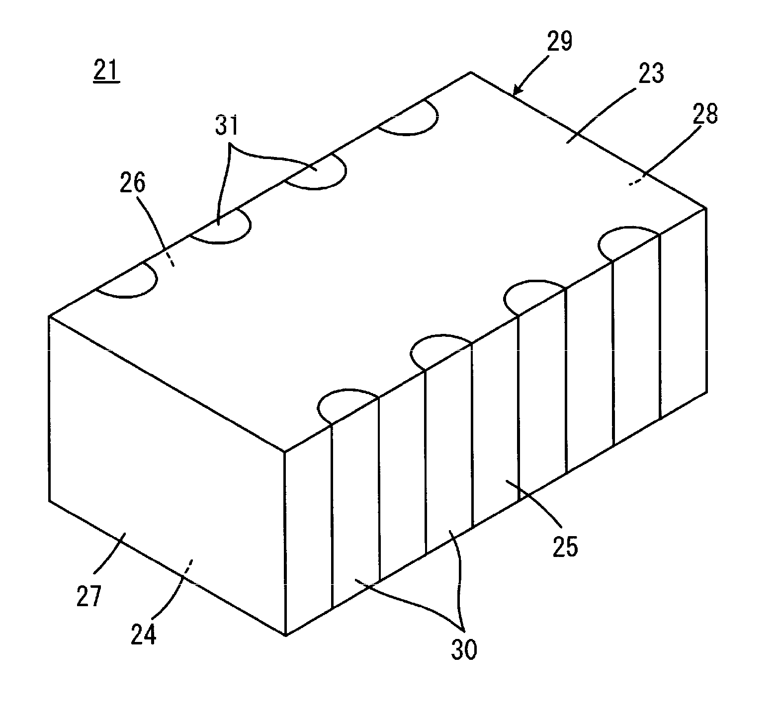
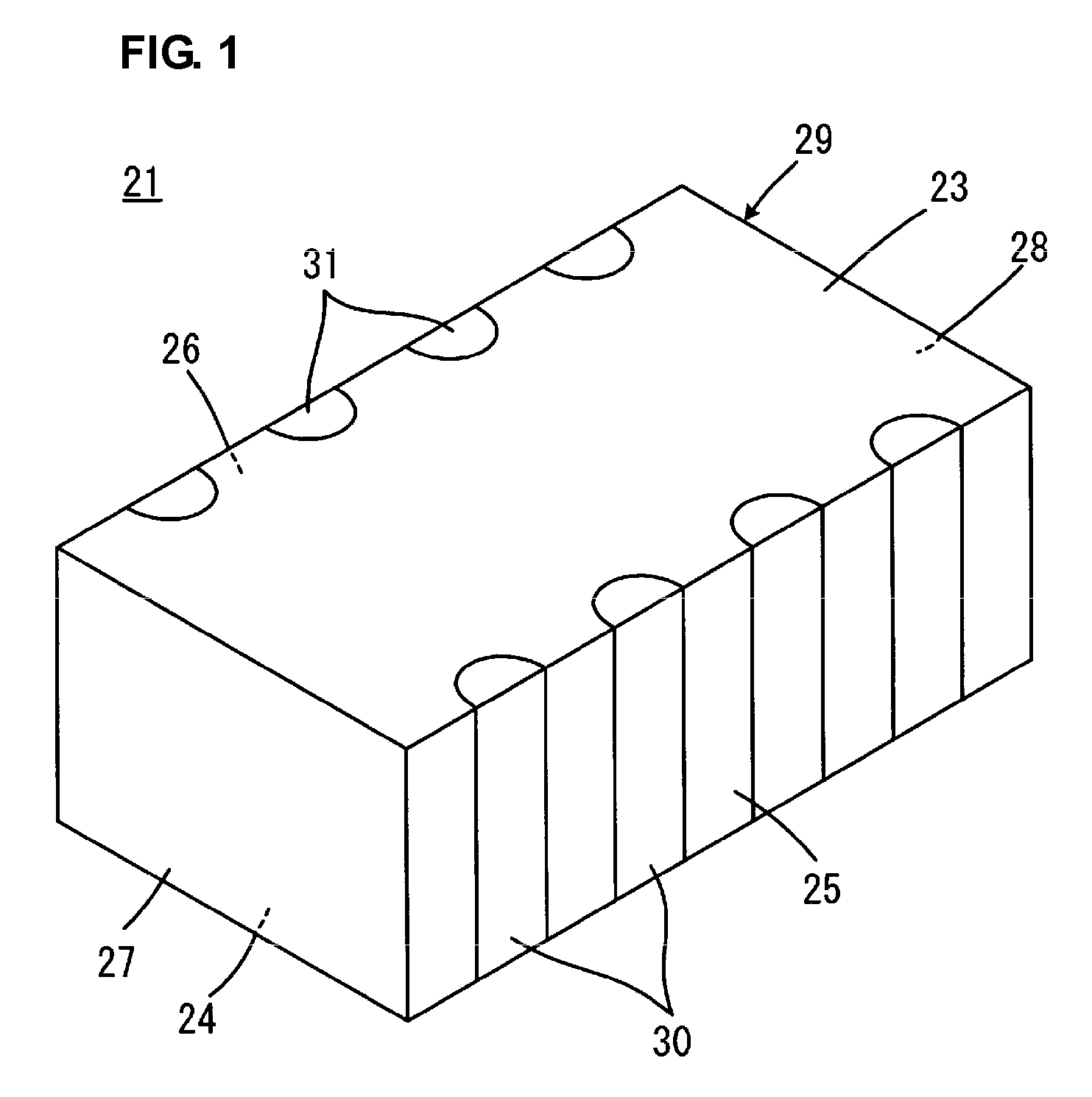
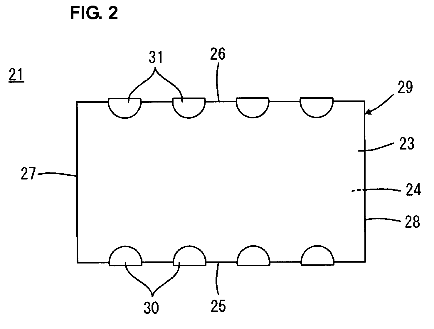
[0042]FIG. 1 is a perspective view of a capacitor array 21 that is an example of a monolithic ceramic electronic component according to a first preferred embodiment of the present invention. FIG. 2 is a plan view of the capacitor array 21. FIGS. 3A and 3B are sectional views of the capacitor array 21 taken along different sections.

[0043]The capacitor array 21 includes a ceramic laminate 29 which includes a plurality of stacked ceramic layers 22 and which preferably has a substantially rectangular parallelepiped shape. The ceramic laminate 29 includes a first principal surface 23, a second principal surface 24 opposed to the first principal surface 23, a first side surface 25, a second side surface 26 opposed to the first side surface 25, a first end surface 27, and a second end surface 28 opposed to the first end surface 27.

[0044]The ceramic layers 22 are preferably made of a dielectric ceramic material preferably including a principal component such as BaTiO3, CaTiO3, SrTiO3, and C...

second preferred embodiment

[0064]FIGS. 5A and 5B show a capacitor array 21a according to a second preferred embodiment of the present invention and correspond to FIGS. 3A and 3B, respectively. In FIGS. 5A and 5B, elements corresponding to those shown in FIG. 3A or 3B are denoted by the same reference numerals as those shown in FIG. 3A or 3B and descriptions thereof are omitted.

[0065]With reference to FIGS. 5A and 5B, in the capacitor array 21a, first internal electrodes 32 and second internal electrodes 33 are alternately arranged in a single plane. According to this configuration, the first lead portions 35 in a specific plane are arranged close to both of a first side surface 25 and the second lead portions 38 in the specific plane are arranged close to a second side surface 26. Thus, junctions between the adjacent ceramic layers 22 are balanced. This allows the capacitor array 21a to have increased reliability.

third preferred embodiment

[0066]FIGS. 6A and 6B show a capacitor array 21b according to a third preferred embodiment of the present invention and correspond to FIGS. 3A and 3B, respectively. In FIGS. 6A and 6B, elements corresponding to those shown in FIG. 3A or 3B are denoted by the same reference numerals as those shown in FIG. 3A or 3B and descriptions thereof are omitted.

[0067]With reference to FIGS. 6A and 6B, in the capacitor array 21b, first projecting portions 36 and second projecting portions 39 have rounded corners 47. This configuration is effective to prevent internal stresses from being concentrated at the corners 47 of the first and second projecting portions 36 and 39.

[0068]First and second projecting portions 36 and 39 of the capacitor array 21a shown in FIGS. 5A and 5B may have rounded corners substantially identical to the corners 47.


PUM

PropertyMeasurementUnit
thicknessaaaaaaaaaa
thicknessaaaaaaaaaa
temperatureaaaaaaaaaa

Abstract

A monolithic ceramic electronic component includes a ceramic laminate which includes a plurality of stacked ceramic layers and which has a first principal surface, a second principal surface opposed to the first principal surface, a first side surface, and a second side surface opposed to the first side surface, first external terminal electrodes arranged on the first side surface, second external terminal electrodes arranged on the second side surface, first internal electrodes arranged in the ceramic laminate, and second internal electrodes arranged in the ceramic laminate. The first internal electrodes include first opposed portions, first lead portions, and first projecting portions. The second internal electrodes include second opposed portions, second lead portions, and second projecting portions.

Description

BACKGROUND OF THE INVENTION[0001]1. Field of the Invention[0002]The present invention relates to monolithic ceramic electronic components, and particularly to a technique to prevent structural defects caused by internal stress from occurring in a monolithic ceramic electronic component.[0003]2. Description of the Related Art[0004]Monolithic ceramic electronic components include ceramic laminates including stacked ceramic layers and internal electrodes extending therebetween. During manufacture of the monolithic ceramic electronic components, each ceramic laminate is prepared using a firing step. In the firing step, the ceramic layers and the internal electrodes are co-fired. Structural defects, such as cracks, may occur in the ceramic laminate in the firing step because of the difference in sintering shrinkage between a ceramic material included in the ceramic layers and a metal included in the internal electrodes. This phenomenon is described below in detail with reference to a mon...

Claims


Application Information

Patent Timeline
Patent Type & Authority Patents(United States)
IPC IPC(8): H01G4/06
CPCH01G4/12H01G4/012
Inventor NAGAMIYA, KATSUMORI
Owner MURATA MFG CO LTD
Why Eureka
Try Eureka