Semiconductor device with NMOS transistors arranged continuously

a technology of nmos transistors and semiconductor devices, which is applied in the direction of semiconductor devices, transistors, electrical equipment, etc., can solve the problems of not being able to use a desired number of nmos transistors among many nmos transistors, and not being able to isolate a desired number of elements,

Active Publication Date: 2009-08-04
RENESAS ELECTRONICS CORP
View PDF5 Cites 104 Cited by
  • Summary
  • Abstract
  • Description
  • Claims
  • Application Information

AI Technical Summary

Problems solved by technology

In recent years, miniaturization of the element has made remarkable progress, and the STI structure stress has become a significant problem.
In this case, it is not possible to use a desired number of NMOS transistors among many NMOS transistors.
In other words, if the diffusion layer length DL is simply elongated, isolation of a desired number of elements is not possible and handling of a desired number of elements is not possible accordingly.

Method used


Image

  • Semiconductor device with NMOS transistors arranged continuously
  • Semiconductor device with NMOS transistors arranged continuously
  • Semiconductor device with NMOS transistors arranged continuously

Examples


first embodiment

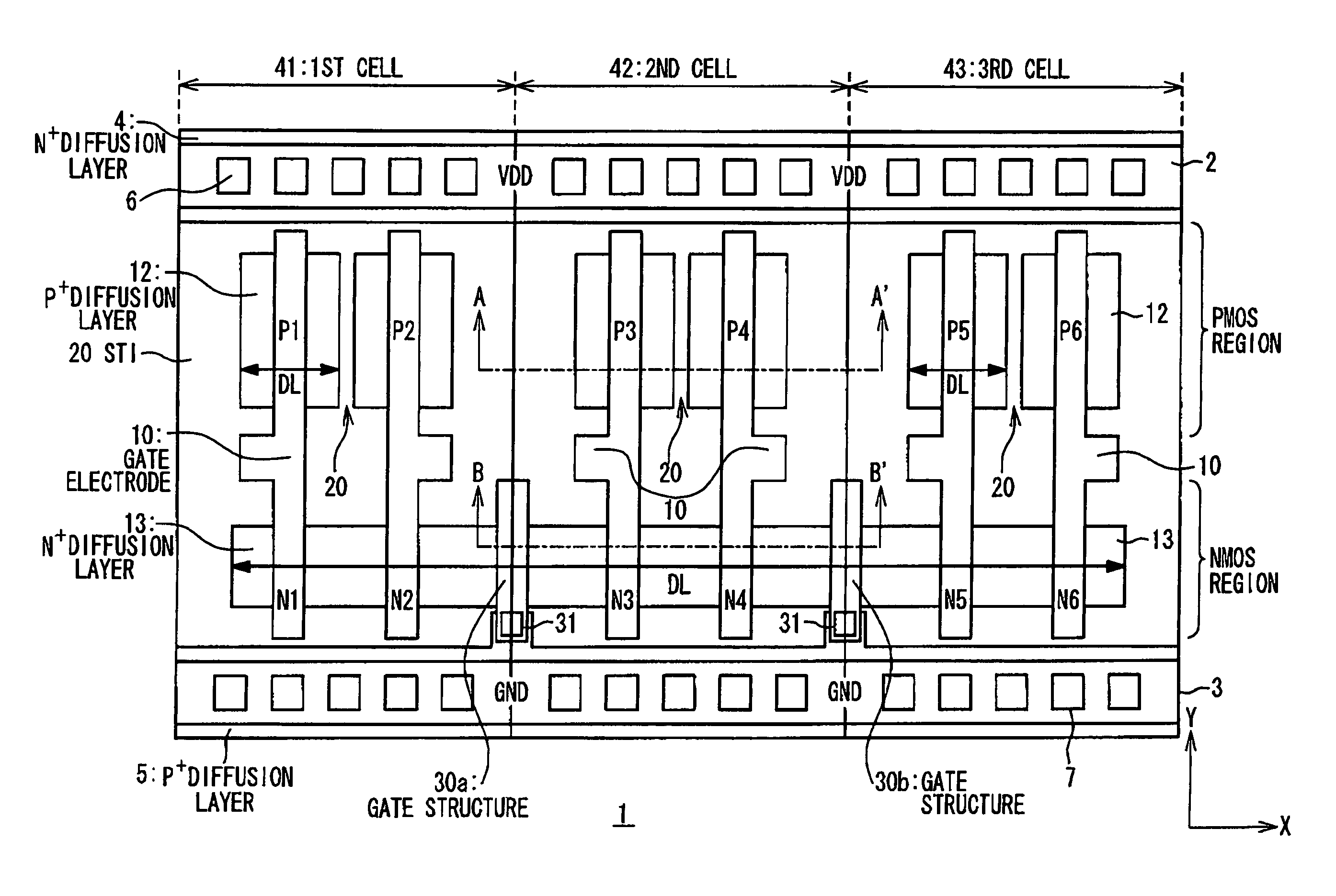
[0040]FIG. 3 is a plan view showing a pattern structure of a semiconductor device 1 according to the first embodiment of the present invention. Referring to FIG. 3, a power supply line 2 for supplying a power supply voltage VDD and a ground line 3 for supplying a ground voltage GND are arranged to extend in an X-direction. The power supply line 2 is connected to an N-type diffusion layer 4 via contacts 6 to apply a power supply voltage as a substrate voltage. Further, the ground line 3 is connected to a P-type diffusion layer 5 via contacts 7 to apply a ground voltage as the substrate voltage. A plurality of PMOS transistors P1 to P6 and a plurality of NMOS transistors N1 to N6 are formed in a region put between the power supply line 2 and the ground line 3. Specifically, the plurality of PMOS transistors P1 to P6 are formed in a PMOS region to be aligned with each other along an X-direction. Also, the plurality of NMOS transistors N1 to N6 are formed in a NMOS region to be aligned ...

second embodiment

[0049]The semiconductor device 1 according to the present invention can be designed by cell-base technique and manufactured. For example, the structure shown in FIG. 3 can be realized by a combination of a first cell 41, a second cell 42 and a third cell 43. The first cell 41 includes PMOS transistors P1 and P2, NMOS transistors N1 and N2 and half of the gate structure 30a. The second cell 42 includes PMOS transistors P3 and P4, NMOS transistors N3 and N4, half of the gate structure 30a and half of the gate structure 30b. The third cell 43 includes PMOS transistors P5 and P6, NMOS transistors N5 and N6 and half of the gate structure 30b. The first cell 41 and the second cell 42 are arranged so that the gate structure 30a is formed when they are adjacent to each other. Further, the second cell 42 and the third cell 43 are arranged so that the gate structure 30b is formed when they are adjacent to each other.

[0050]Further, the semiconductor device 1 according to the present invention ...

third embodiment

[0058]FIG. 8A shows an example of wirings to be used for the structure of inverters as the semiconductor device according to the third embodiment of the present invention. A source of the PMOS transistor P1 is connected to a power supply line by a wiring 61. A source of the PMOS transistor P2 is connected to the power supply line by a wiring 62. A source of the NMOS transistor N1 is connected to a ground line by a wiring 63. A source of the NMOS transistor N2 is connected to the ground line by a wiring 64. A drain of the PMOS transistor P1 is connected to a drain of the NMOS transistor N1 by a wiring 65. A drain of the PMOS transistor P2 is connected to a drain of the NMOS transistor N2 by a wiring 66. Further, the wiring 65 and the wiring 66 are connected to each other. Further, a gate electrode 10-1 of the PMOS transistor P1 and the NMOS transistor N1, and a gate electrode 10-2 of the PMOS transistor P2 and the NMOS transistor N2 are connected via a wiring 67. With this configurat...


PUM


Abstract

A semiconductor device includes a plurality of PMOS transistors formed on a semiconductor substrate; and a plurality of NMOS transistors formed on the semiconductor substrate. The plurality of PMOS transistors are electrically isolated from each other by a device isolation structure formed in the semiconductor substrate. The plurality of NMOS transistors are continuously formed in a first direction such that a sequence of N-type diffusion layers of the plurality of NMOS transistors extends in the first direction. One of the plurality of PMOS transistors and one of the plurality of NMOS transistors share a gate electrode.

Description

BACKGROUND OF THE INVENTION[0001]1. Field of the Invention[0002]The present invention relates to a semiconductor device. More particularly, the present invention relates to a semiconductor device including PMOS transistors and NMOS transistors, and a manufacturing method of the same.[0003]2. Description of the Related Art[0004]It is indispensable in designing an LSI (Large-Scaled Integrated Semiconductor Device) to use a computer for the sake of reduction in time for designing and confirmation and to eliminate man-caused mistakes. A semiconductor device design supporting system using the computer in this manner is referred to as a CAD (Computer Aided Design) system. According to a LSI designing method of cell base, cells of a plurality of types are configured as a library. A designer executes designing of LSI by utilizing CAD and allocating a desired cell in a layout space defined on the computer.[0005]FIG. 1 shows basic cells (primitive cells) for designing a conventional semicondu...

Claims


Application Information

Patent Timeline
Patent Type & Authority Patents(United States)
IPC IPC(8): H01L27/092
CPCH01L27/0207H01L29/4238H01L27/11807H01L27/092
Inventor SUZUKI, FUMIAKI
Owner RENESAS ELECTRONICS CORP
Why Eureka
Try Eureka