Method of producing a solar cell; a solar cell and a method of producing a semiconductor device

a solar cell and solar cell technology, applied in the field of solar cell and semiconductor device production, can solve the problem of remarkable reduction of the energy conversion efficiency of the solar cell

Inactive Publication Date: 2000-07-25
MITSUBISHI ELECTRIC CORP
View PDF11 Cites 100 Cited by
  • Summary
  • Abstract
  • Description
  • Claims
  • Application Information

AI Technical Summary

Problems solved by technology

As a result, the energy conversion efficiency of the solar cell is remarkably reduced.

Method used


Image

  • Method of producing a solar cell; a solar cell and a method of producing a semiconductor device
  • Method of producing a solar cell; a solar cell and a method of producing a semiconductor device
  • Method of producing a solar cell; a solar cell and a method of producing a semiconductor device

Examples


embodiment 2

FIGS. 4a to 4f depict the steps in a manufacturing process of a solar cell and a structure of solar cell with respect to Embodiment 2 of the present invention. The manufacturing process will be described with reference to FIGS. 4a to 4f.

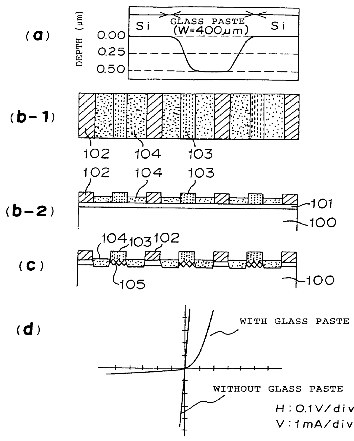
FIG. 4a shows a state that a pattern of a glass paste 104 is formed on a p type silicon substrate 100 in which an n type diffusion layer 101 is formed in the same manner as Embodiment 1. FIG. 4b shows a state that the glass paste 104 is removed by etching after a sample shown in FIG. 4a has been baked. The n type diffusion layer 101 is removed in accordance with the mechanism described with respect to Embodiment 1, and a surface of a p type silicon substrate 106 is exposed as shown in FIG. 4b.

FIG. 4c shows that an n electrode 102 of a silver paste is formed on the n type diffusion layer 101 which is not subjected to the patterning of the glass paste 104 and a p electrode 103 of an aluminum-silver paste is formed on the surface of the p type silicon s...

embodiment 1

The electrodes 102, 103 and 107 may be baked separately. However, the electrodes 102, 103 and 107 can be baked simultaneously after they have been printed in a continuous manner so that the manufacturing process can be simplified. The n type diffusion layer 101 to be formed on the main light incident plane can be formed by various ways as described with respect to The order of formation can be changed, specifically, the n type diffusion layer 101 to be formed on the main light incident plane may be formed simultaneously or after the formation of the n type diffusion layer 101 to be formed on the rear plane.

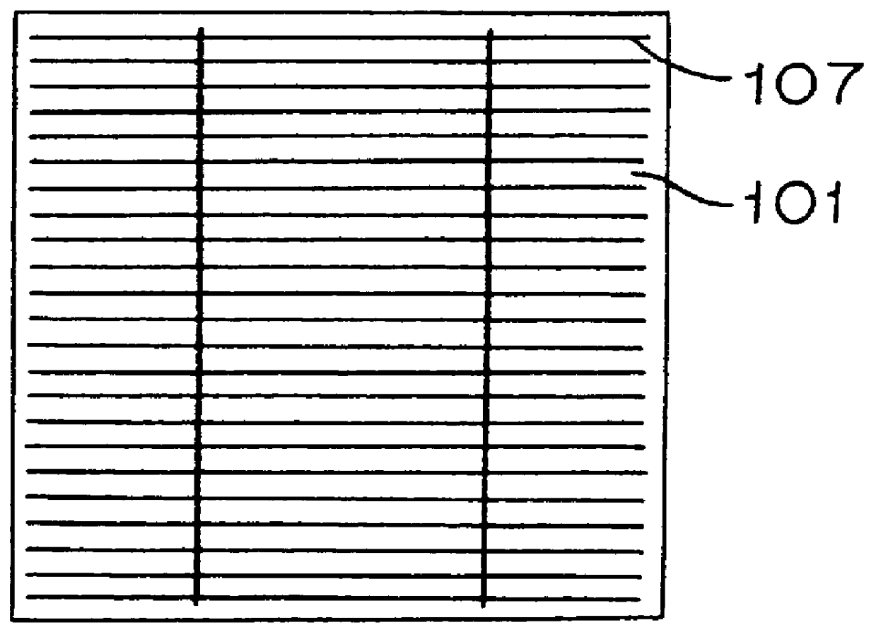
FIGS. 4e and 4f show models of electrode pattern for the solar cell. The solar cell shown in FIGS. 4e and 4f has such structure that the n electrode 107 is provided on the main light incident plane and the n electrode 102 and the p electrode 103 are provided on the rear plane (opposite plane), which is known as one of effective structures to improve the conversion efficiency of t...

embodiment 3

FIGS. 5a-d are diagram for explaining a manufacturing method of Embodiment 3 to realize the structure of the solar cell of Embodiment 2.

In Embodiment 2, description has been made as to the method of removing the glass paste 104 in order to electrically separate the p n junction. However, as already described with respect to Embodiment 1, it is not always necessary to remove the glass paste 104. In this embodiment, description will be made as to a case of manufacturing process of solar cell in which the glass paste 104 is not removed.

FIG. 5a shows a state that a silver paste pattern for an n electrode 102 and an aluminum-silver paste pattern for a p electrode 103 are formed by printing on the p type silicon substrate 100 in which the n type diffusion layer 101 is formed in the same manner as Embodiment 1, and the substrate 100 with the patterns is baked, wherein reference numeral 105 designates a p type inversion layer which is the same as already described.

FIG. 5b shows a state that...


PUM

PropertyMeasurementUnit
thicknessaaaaaaaaaa
thicknessaaaaaaaaaa
thickaaaaaaaaaa

Abstract

A solar cell and a method of producing the same which realizes electrical separation of the p n junction in a simple manner, and a method of producing a semiconductor device a method of producing a semiconductor device in which an electrode is formed by using a metallic paste material on a substrate covered with a silicon nitride film or a titanium oxide film, wherein a glass paste 104 composed mainly of glass which has a property of melting silicon is provided on an n type diffusion layer 101 in the p n junction; the substrate is baked so that penetration of the n type diffusion layer 101 is effected by the glass paste; aluminum is diffused in the n type diffusion layer 101 below a p electrode 103 formed of an aluminum silver paste to thereby form a p type inversion layer 105 inverted to a p type, whereby the electrical separation of the p n junction can be realized. Further, when a metallic paste material is provided on an insulating film and the metallic paste material is baked, the material penetrates the insulating film to electrically contact with the semiconductor substrate.

Description

1. Field of the InventionThe present invention relates to a method of producing a solar cell; a solar cell, and a method of producing a semiconductor device. In particular, it relates to a method of producing a silicon solar cell which realizes electrical separation of the p n junction necessary for forming the electrodes easily and with a high productivity; a solar cell having the p n junction which is electrically separated in a simple manner, and a method of producing a semiconductor device in which the electrode capable of reducing substantially the contact resistance to the semiconductor substrate by applying the same physical phenomenon as in the electrical separation of the p n junction in forming the electrodes of the solar cell.2. Discussion of BackgroundNow, silicon solar cells form the main stream for power solar cells on the earth. In general, process flows in large scale production have to be simple as possible to reduce manufacturing cost.In the following, description ...

Claims


Application Information

Patent Timeline
Patent Type & Authority Patents(United States)
IPC IPC(8): H01L31/0216H01L31/0224H01L31/18H01L31/04
CPCH01L31/02168H01L31/022425H01L31/1804H01L31/022441H01L31/022458H01L31/068H01L31/0682Y02E10/547
Inventor ARIMOTO, SATOSHI
Owner MITSUBISHI ELECTRIC CORP
Why Eureka
Try Eureka