Semiconductor device

a technology of semiconductor devices and semiconductors, applied in the direction of semiconductor devices, semiconductor/solid-state device details, diodes, etc., can solve the problems of gate insulating film breaking down, electric field applied, gate insulating film being destroyed

Inactive Publication Date: 2005-12-08
KK TOSHIBA
View PDF4 Cites 92 Cited by
  • Summary
  • Abstract
  • Description
  • Claims
  • Application Information

AI Technical Summary

Problems solved by technology

Thereby, there is a possibility that an excessive electric field is applied to a gate insulating film and the gate insulating film is destroyed.
Further, after the semiconductor device is completed, there is a possibility that the gate insulating film is broken down by human electrostatic discharge (ESD), for example.

Method used


Image

  • Semiconductor device
  • Semiconductor device
  • Semiconductor device

Examples


first reference example

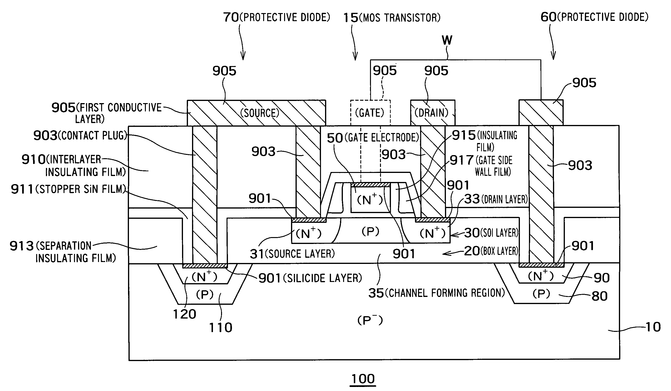
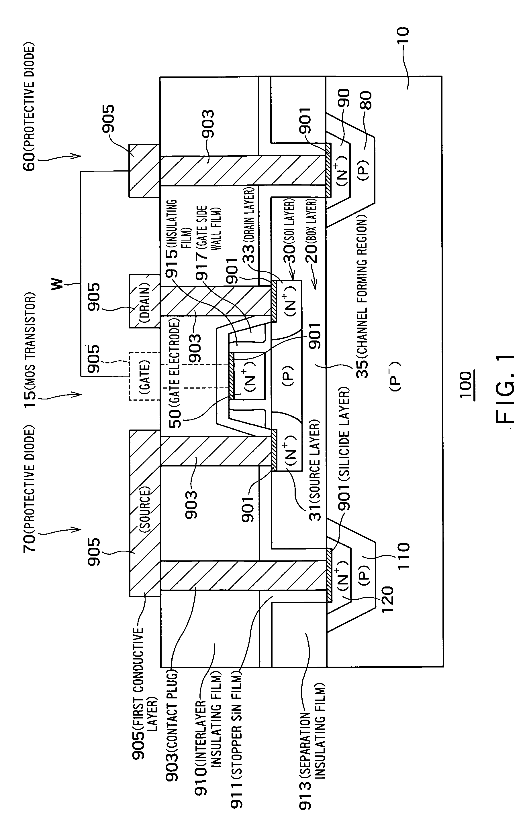
[0026]FIG. 1 is a sectional view of a semiconductor device 100 according to a first reference example according to the invention. The semiconductor device 100 is formed on an SOI substrate having a P−-type semiconductor substrate 10 consisting of silicon, an embedded insulating layer (hereinafter, referred to as “BOX layer”) 20 provided on the semiconductor substrate 10, and a semiconductor layer (hereinafter, referred to as “SOI layer”) 30 provided on the BOX layer 20.

[0027] The semiconductor device 100 includes an N-type channel MOS transistor 15 formed on the SOI substrate. The MOS transistor 15 has an N+-type source layer 31 and an N+-type drain layer 33 within the SOI layer 30. A channel forming region 35 is provided between the source layer 31 and the drain layer 33. On the channel forming region 35, a gate electrode 50 is formed via a gate insulating film 40.

[0028] The source layer 31 is electrically connected to an embedded insulating layer protective diode 70 (hereinafter...

second reference example

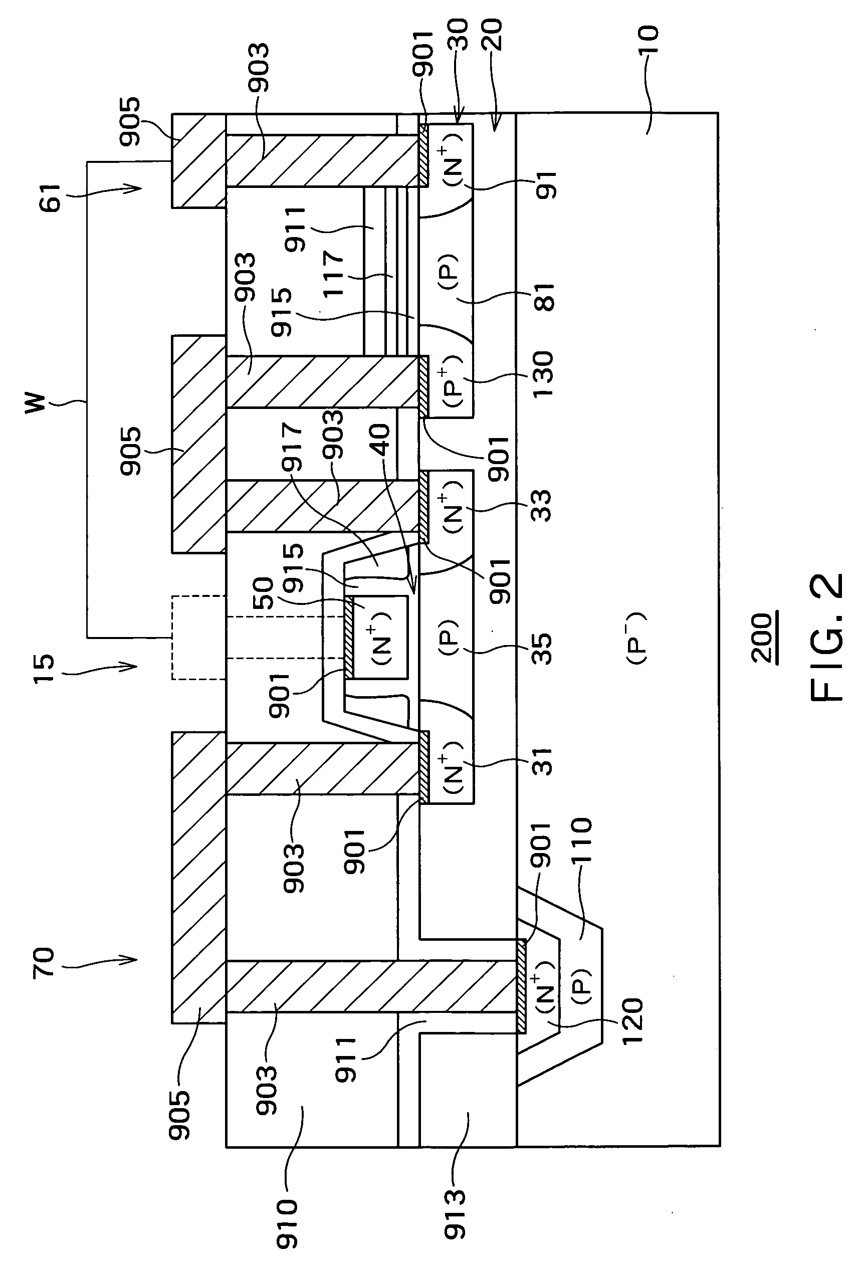
[0037]FIG. 2 is a sectional view of a semiconductor device 200 according to a second reference example according to the invention. The second reference example is different from the first reference example on the point that a gate insulating film protective diode 61 is formed in the SOI layer 30.

[0038] The protective diode 61 has a P-type third diffusion layer 81 and an N+-type fourth diffusion layer 91. The third diffusion layer 81 is formed within the SOI layer 30, and the fourth diffusion layer 91 is formed within the SOI layer 30 so as to be adjacent to the third diffusion layer 81. Furthermore, the protective diode 61 has a P+-type contact layer 130 so as to electrically connect the third diffusion layer 81 and the drain layer 33.

[0039] Silicide layers 901 are provided on the contact layer 130. Contact plugs 903 are provided on the silicide layers 901. The contact layer 130 and the drain layer 33 are electrically connected each other by the first conductive layers 905 via the...

third reference example

[0043]FIG. 3 is a sectional view of a semiconductor device 300 according to a third reference example according to the invention. The third reference example is different from the first reference example on the point that an embedded insulating layer protective diode 71 is formed in the SOI layer 30.

[0044] The protective diode 71 has a P-type first diffusion layer 111 formed within the SOI layer 30 and an N+-type second diffusion layer 121 formed within the SOI layer 30 so as to be adjacent to the first diffusion layer 111. Furthermore, the protective diode 71 has a P+-type contact layer 140 within the SOI layer 30 and a P+-type contact layer 150 in the semiconductor substrate 10 so as to electrically connect the first diffusion layer 111 and the semiconductor substrate 10 each other.

[0045] Silicide layers 901 are provided on the second diffusion layer 121, the contact layer 140 and the contact layer 150. Contact plugs 903 are provided on the silicide layers 901. The second diffus...


PUM


Abstract

A semiconductor device comprises a semiconductor substrate; an embedded insulating layer provided on the semiconductor substrate; a semiconductor layer provided on the embedded insulating layer; a transistor including a first conductivity type source layer formed within the semiconductor layer, a first conductivity type drain layer formed in the semiconductor layer, and a channel forming region between the source layer and the drain layer; and an embedded insulating layer protective diode including a second conductivity type first diffusion layer and a first conductivity type second diffusion layer, the first diffusion layer being at the same potential as a semiconductor substrate region immediately below the channel forming region, the second diffusion layer being provided adjacently to the first diffusion layer and electrically connected to at least one of the source layer, the drain layer and the channel forming region.

Description

CROSS-REFERENCE TO RELATED APPLICATIONS [0001] This application is based upon and claims the benefit of priority from the prior Japanese Patent Applications No. 2004-165789, filed on Jun. 3, 2004, the entire contents of which are incorporated herein by reference. BACKGROUND OF THE INVENTION [0002] 1. Field of the Invention [0003] The present invention relates to a semiconductor device. [0004] 2. Background Art [0005] Recently, with miniaturization and complication of a semiconductor device, a multilayer interconnection structure is adopted. In order to form the multilayer interconnection structure, it is necessary to repeatedly perform plasma CVD (Chemical Vapor Deposition), RIE (Reactive Ion Etching) or the like on a MOS transistor. Since these treatments are for performing deposition or etching utilizing electrical polarities, a gate electrode and a substrate are charged. Thereby, there is a possibility that an excessive electric field is applied to a gate insulating film and the ...

Claims


Application Information

Patent Timeline
Patent Type & Authority Applications(United States)
IPC IPC(8): H01L27/04H01L21/822H01L21/8234H01L27/02H01L27/06H01L27/08H01L27/088H01L27/10H01L27/12H01L29/786
CPCH01L27/0255H01L27/1203H01L29/7841H01L2924/0002H01L2924/00
Inventor MINAMI, YOSHIHIRO
Owner KK TOSHIBA
Why Eureka
Try Eureka