Methods and systems for utilizing design data in combination with inspection data

a technology of design data and inspection data, applied in the field of methods and systems for utilizing design data in combination with inspection data, can solve the problems of affecting the electrical parameters of the device, the operation of semiconductor manufacturing processes closer to the limitation of the performance capability of the process, and the need for detachment of defects of decreasing size, etc., to achieve the effect of improving one or more defect capture rates

Active Publication Date: 2009-08-04
KLA TENCOR TECH CORP
View PDF329 Cites 426 Cited by
  • Summary
  • Abstract
  • Description
  • Claims
  • Application Information

AI Technical Summary

Benefits of technology

[0051]It is noted that alignment accuracy depends on both coordinate transformation from design to wafer and coordinate accuracy of the inspection system. Preferably, therefore, the coordinates reported by the inspection system are substantially accurate. In addition, the measurements for alignment sites may be performed using logical inspection coordinates. (Inspection systems output logical wafer coordinates, but defect review tools such as scanning electron microscopes (SEMs) measure physical wafer coordinates. Therefore, the physical coordinates on the wafer may be corrected by the inspection system to account for difference in reticle offset scaling and slight rotation when compared to the expected wafer layout. As such, these corrections may also be applied to the SEM measurements to reduce errors between the two coordinate systems from reticle to reticle.)
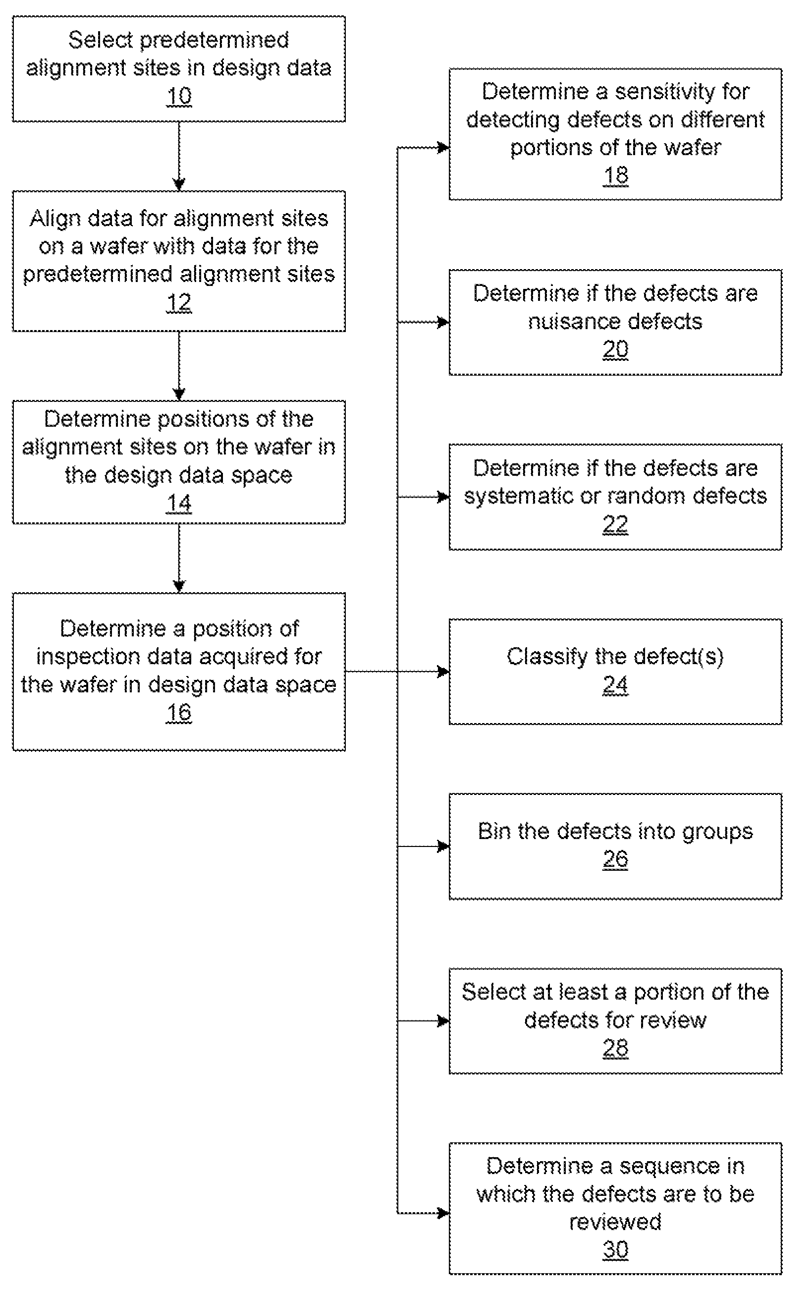
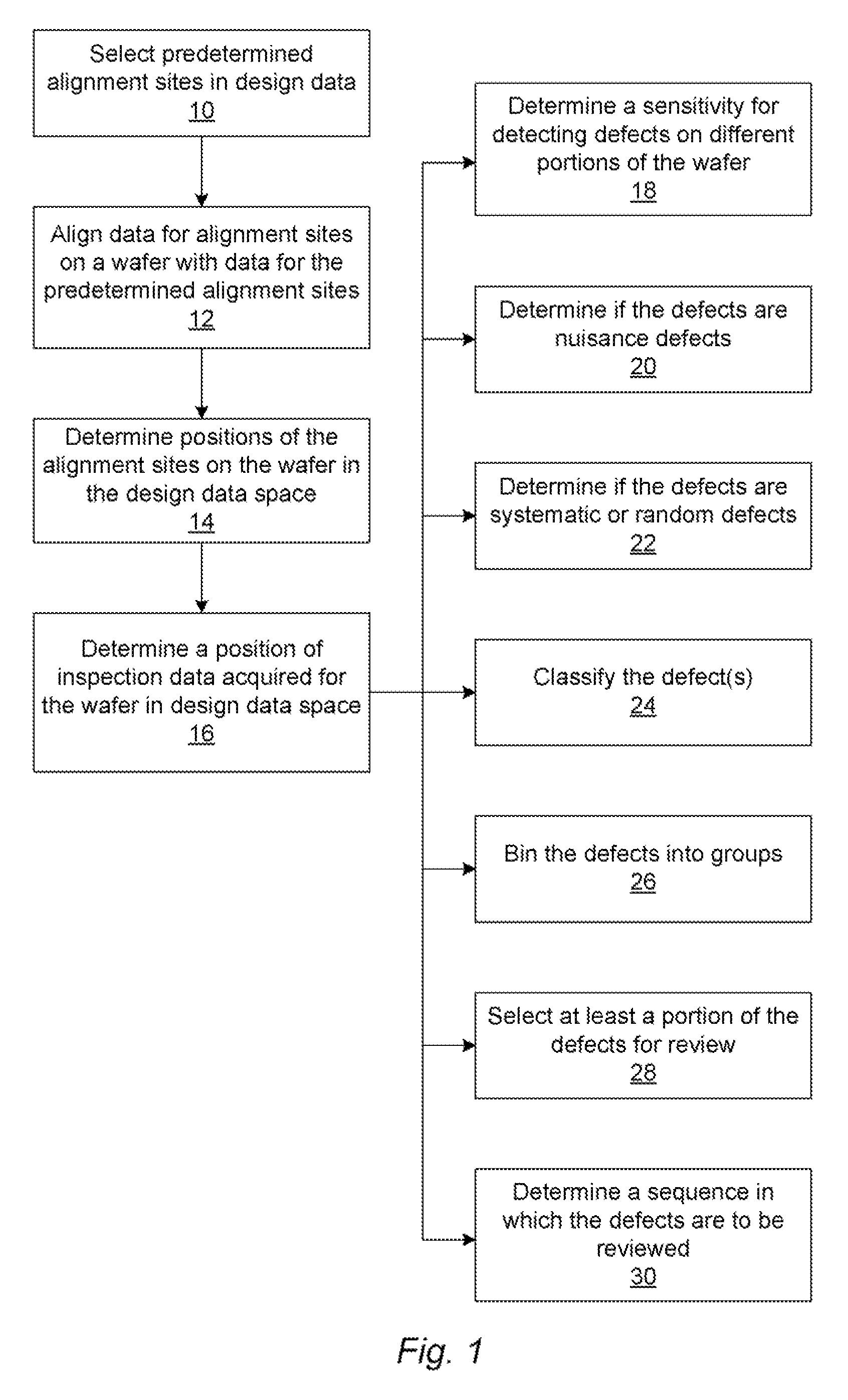
[0057]In yet another embodiment, the defects were detected by an inspection process, and the method includes reviewing locations on the wafer at which one or more patterns of interest (POIs) in the design data are printed, determining based on results of the reviewing step if defects should have been detected at the locations of the one or more POIs, and altering the inspection process to improve one or more defect capture rates.
[0060]In some embodiments, the method includes determining if one or more of the groups of defects correspond to nuisance defects by reviewing at least some of the defects in the one or more of the groups and removing the one or more of the groups corresponding to the nuisance defects from results of an inspection process in which the defects were detected to increase signal-to-noise ratio of the results of the inspection process. In another embodiment, the method includes classifying one or more of the groups of defects based on results of review of at least some of the defects in the one or more of the groups, one or more attributes of design data, one or more attributes of the defects, or some combination thereof. In an additional embodiment, the method includes determining a root cause of one or more of the groups of defects based on results of review of at least some of the defects in the one or more of the groups, one or more attributes of the design data, one or more attributes of the defects, or some combination thereof.
[0112]In one embodiment, the defects were detected by an inspection process, and the method includes reviewing locations on the wafer at which one or more POIs in the design data are printed, determining based on results of the reviewing step if defects should have been detected at the locations of the one or more POIs, and altering the inspection process to improve one or more defect capture rates.
[0118]In one embodiment, the method includes determining if the defects are nuisance defects based on the DBCs assigned to the defects and removing the nuisance defects from results of an inspection process in which the defects were detected to increase signal-to-noise ratio of the results of the inspection process.
[0134]A further embodiment relates to a method for altering an inspection process for wafers. The method includes reviewing locations on the wafer at which one or more POIs in the design data are printed. The method also includes determining based on results of the reviewing step if defects should have been detected at the locations of the one or more POIs. In addition, the method includes altering the inspection process to improve one or more defect capture rates for defects located in at least some of the one or more POIs.

Problems solved by technology

However, as the dimensions of semiconductor devices decrease, inspection becomes even more important to the successful manufacture of acceptable semiconductor devices because smaller defects can cause the devices to fail.
For instance, as the dimensions of semiconductor devices decrease, detection of defects of decreasing size has become necessary since even relatively small defects may cause unwanted aberrations in the semiconductor devices.
As design rules shrink, however, semiconductor manufacturing processes may be operating closer to the limitation on the performance capability of the processes.
In addition, smaller defects can have an impact on the electrical parameters of the device as the design rules shrink, which drives more sensitive inspections.
Therefore, as design rules shrink, the population of potentially yield relevant defects detected by inspection grows dramatically, and the population of nuisance defects detected by inspection also increases dramatically.
Therefore, more and more defects may be detected on the wafers, and correcting the processes to eliminate all of the defects may be difficult and expensive.
Furthermore, at smaller design rules, process induced failures may, in some cases, tend to be systematic.
That is, process induced failures tend to fail at predetermined design patterns often repeated many times within the design.
Whether or not defects will affect device parameters and yield often cannot be determined from the inspection, review, and analysis processes described above since these processes may not be able to determine the position of the defect with respect to the electrical design.
However, currently the care areas can be aligned to the pattern printed on the wafer with an accuracy of no better than about 2 μm due to system errors and imperfections.
In addition, the inspection care areas in currently used methods are relatively large and include many non-critical features as well as desired critical features.
In trying to maximize the sensitivity of the inspection system to capture subtle spatially systematic “design-for-manufacturability” (DFM) defects resulting from design and process interdependencies, the system may be overwhelmed by millions of events in non-critical areas such as CMP fill regions.
Detecting such nuisance defects is disadvantageous for a number of reasons.
In addition, nuisance event detection limits the ultimate achievable sensitivity of the inspection system for DFM applications.
A high rate of nuisance defect data may also overload the run time data processing capacity of the inspection system thereby reducing throughput and / or causing the loss of data.

Method used


Image

  • Methods and systems for utilizing design data in combination with inspection data
  • Methods and systems for utilizing design data in combination with inspection data
  • Methods and systems for utilizing design data in combination with inspection data

Examples


Embodiment Construction

[0175]As used herein, the term “wafer” generally refers to substrates formed of a semiconductor or non-semiconductor material. Examples of such a semiconductor or non-semiconductor material include, but are not limited to, monocrystalline silicon, gallium arsenide, and indium phosphide. Such substrates may be commonly found and / or processed in semiconductor fabrication facilities.

[0176]A wafer may include one or more layers formed upon a substrate. For example, such layers may include, but are not limited to, a resist, a dielectric material, and a conductive material. Many different types of such layers are known in the art, and the term wafer as used herein is intended to encompass a wafer including all types of such layers.

[0177]One or more layers formed on a wafer may be patterned or unpatterned. For example, a wafer may include a plurality of dies, each having repeatable patterned features. Formation and processing of such layers of material may ultimately result in completed de...


PUM


Abstract

Various methods and systems for utilizing design data in combination with inspection data are provided. One computer-implemented method for binning defects detected on a wafer includes comparing portions of design data proximate positions of the defects in design data space. The method also includes determining if the design data in the portions is at least similar based on results of the comparing step. In addition, the method includes binning the defects in groups such that the portions of the design data proximate the positions of the defects in each of the groups are at least similar. The method further includes storing results of the binning step in a storage medium.

Description

PRIORITY CLAIM[0001]This application claims priority to U.S. Provisional Application Nos. 60 / 737,947 entitled “Methods and Systems for Utilizing Design Data in Combination with Inspection Data,” filed Nov. 18, 2005, and 60 / 738,290 entitled “Methods and Systems for Utilizing Design Data in Combination with Inspection Data,” filed Nov. 18, 2005, which are incorporated by reference as if fully set forth herein.BACKGROUND OF THE INVENTION[0002]1. Field of the Invention[0003]The present invention generally relates to methods and systems for utilizing design data in combination with inspection data. Certain embodiments relate to a computer-implemented method for determining a position of inspection data in design data space and / or substantially accurately determining the position of a design space location on a wafer during an inspection process.[0004]2. Description of the Related Art[0005]The following description and examples are not admitted to be prior art by virtue of their inclusion...

Claims


Application Information

Patent Timeline
Patent Type & Authority Patents(United States)
IPC IPC(8): G06K9/00
CPCG06F17/5081G03F1/84G06F30/398G06T7/0006G06T7/0008G06T2207/20076G06T2207/30148
Inventor ZAFAR, KHURRAMKEKARE, SAGARCHANG, ELLISPARK, ALLENROSE, PETER
Owner KLA TENCOR TECH CORP
Why Eureka
Try Eureka