
Circuit structure with a double-gate organic thin film transistor device and application thereof

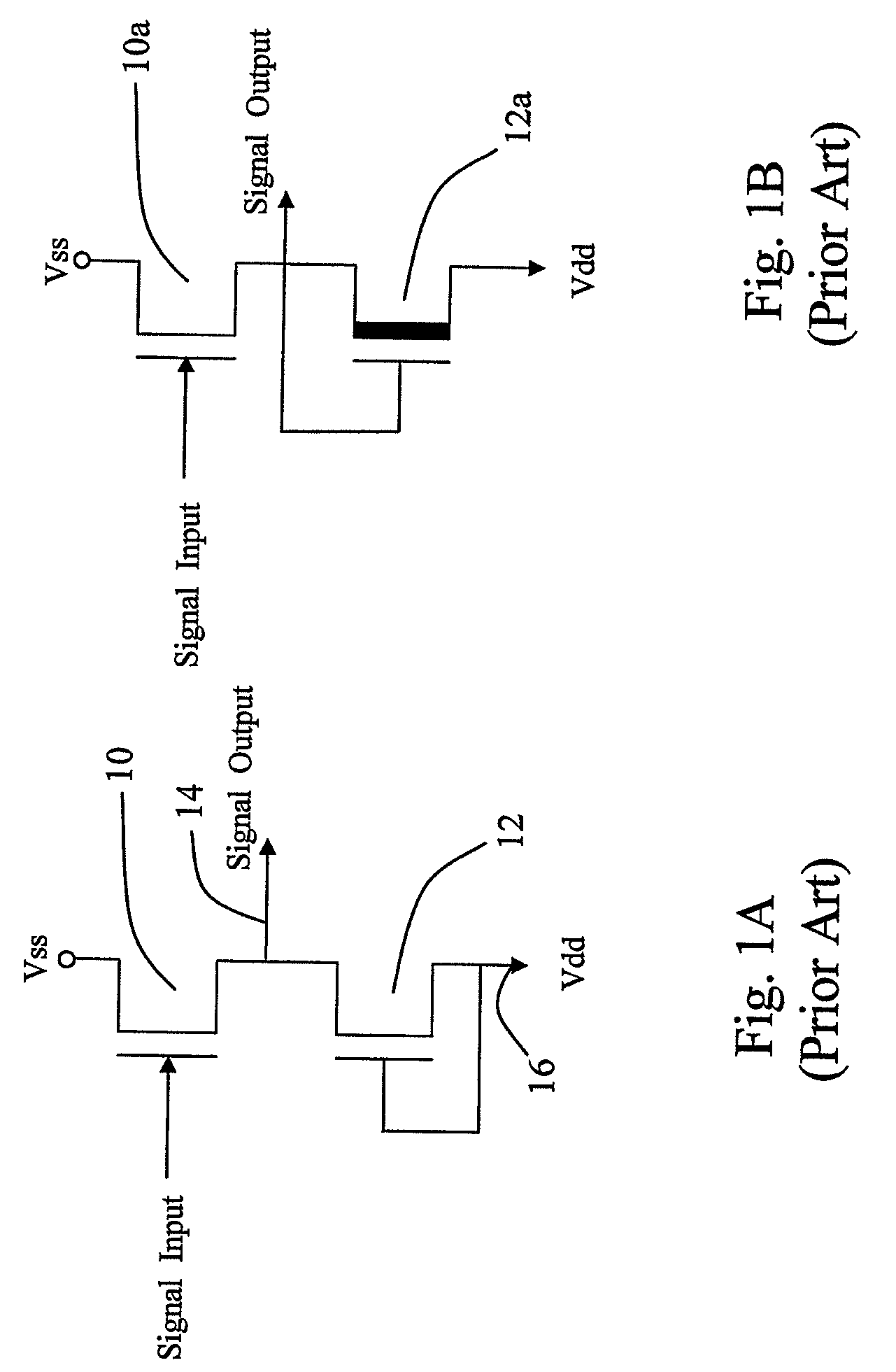
a transistor device and circuit structure technology, applied in the direction of thermoelectric device junction materials, semiconductor devices, electrical apparatus, etc., can solve the problems of increased signal distortion, reduced signal transmission accuracy, and inability to control the threshold voltage of the transistor device, so as to improve the signal transmission accuracy

Active Publication Date: 2009-09-01
IND TECH RES INST
View PDF2 Cites 0 Cited by
  • Summary
  • Abstract
  • Description
  • Claims
  • Application Information

AI Technical Summary

Benefits of technology

[0006]One objective of the present invention is to provide a circuit structure with a double-gate organic thin film transistor device, in which the characteristic of the double-gate organic thin film transistor is advantageously changed by the double-gate structure, and hence improving accuracy of signal transmission.
[0009]In the double-gate structure formed of the first gate and second gate, a threshold voltage of the double-gate organic thin film transistor is a sum of respective voltages of the first gate and second gate. As such, by adjusting one of the two gate voltages the threshold voltage of another gate can be reduced.
[0010]Moreover, the present invention can change the characteristic of the organic thin film transistor to become an enhanced-type transistor or a depletion-type transistor by adjusting the threshold voltage of the second gate.
[0012]The double-gate thin film transistor device can become a depletion-type N channel transistor by adjusting the bias voltage of the second gate terminal so as to improve the accuracy of signal transmission of the circuit structure. As such, the circuit structure can be designed to become an inverter with an enhanced-type N channel transistor and a depletion-type N channel transistor.

Problems solved by technology

Because there is no any doping process involved in the manufacture of the current organic thin film transistor, the threshold voltage of the transistor device can not be controlled.
Due to the large threshold voltage of the organic thin film transistor, the signal distortion is more severe.
As a consequence, the switch elements of the pixel area will make mal-operation.

Method used


Image

  • Circuit structure with a double-gate organic thin film transistor device and application thereof
  • Circuit structure with a double-gate organic thin film transistor device and application thereof
  • Circuit structure with a double-gate organic thin film transistor device and application thereof

Examples


Embodiment Construction

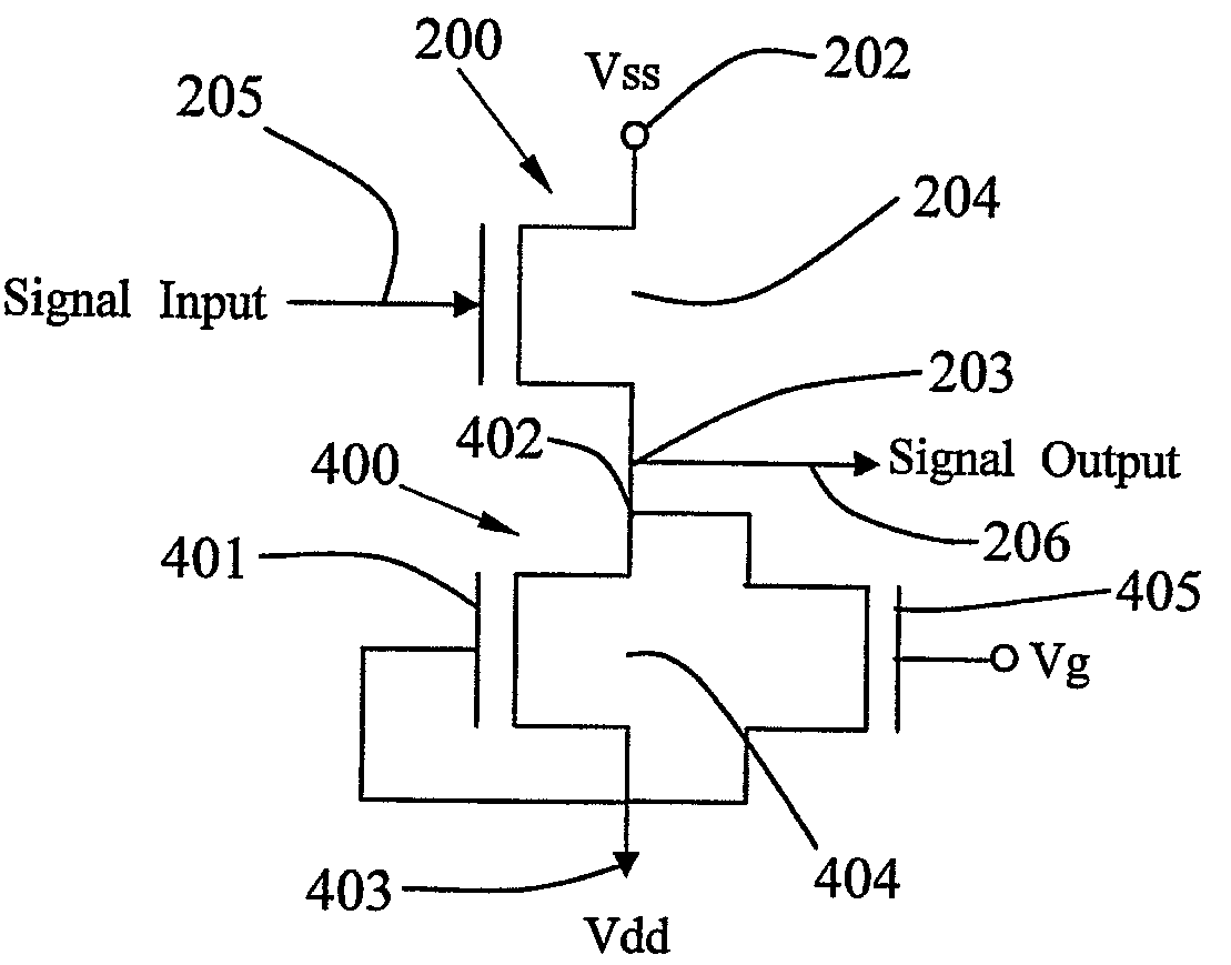
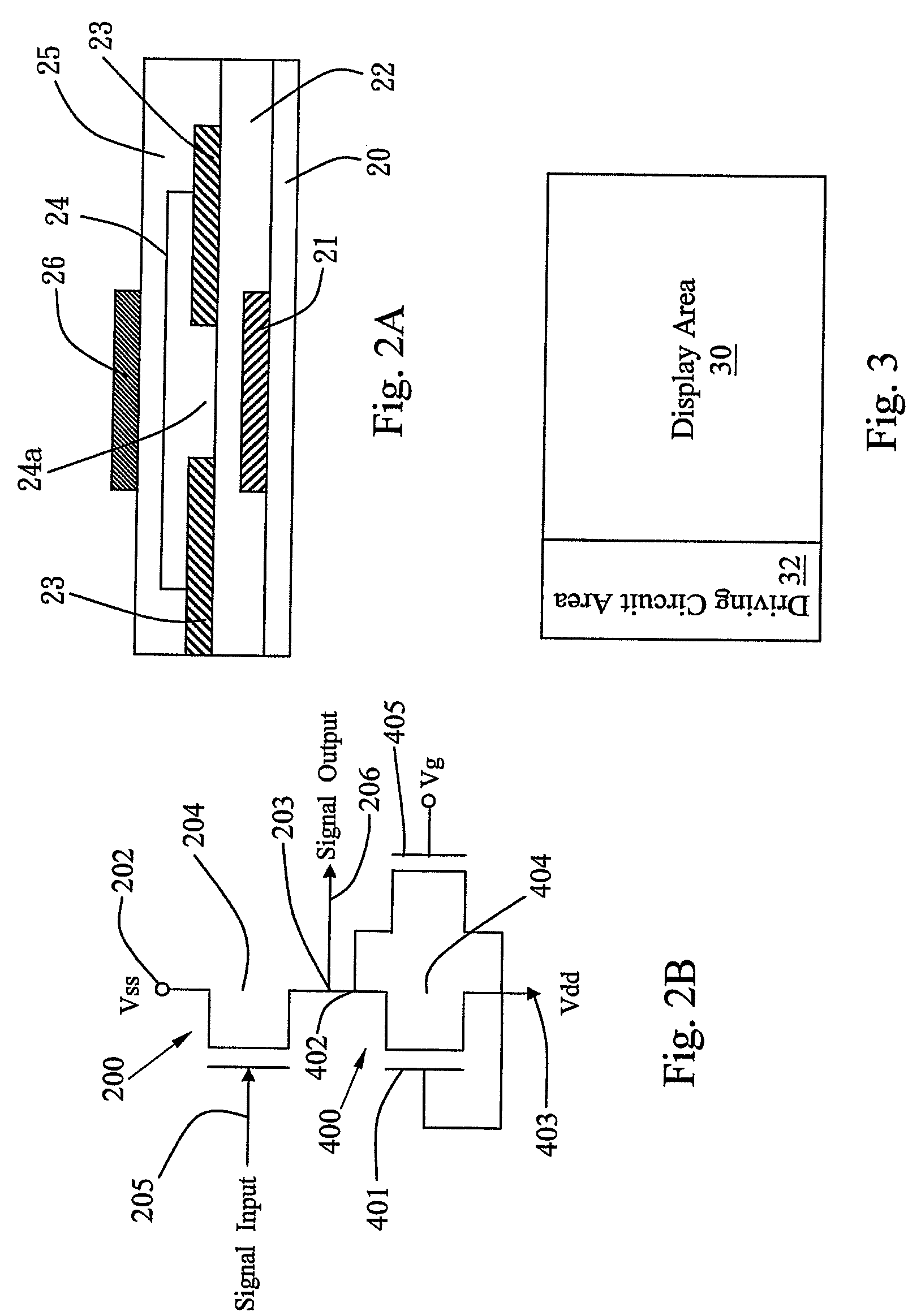
[0021]The present invention forms a protection layer on an organic thin film transistor with a bottom gate so as to use the protection layer as another gate insulating layer. And a metal layer is formed on the protection layer to serve as another gate to accomplish a double-gate organic thin film transistor structure. In the double-gate organic thin film transistor structure, the double gates share a pair of source and drain as well as an organic semiconductor channel area. A threshold voltage of the organic thin film transistor is a sum of the threshold voltages of the first gate and second gate. As such, by the double gate structure the threshold voltage of the organic thin film transistor can be adjustably decreased. Moreover, the organic thin film transistor can become a depletion-type transistor or an enhanced-type transistor by controlling the bias voltage of the second gate. The present invention can adopt the above double gate structure in a particular circuit design, and mo...


PUM


Abstract

This invention provides a circuit structure with a double-gate organic thin film transistor device and application thereof. A protection layer covered on an organic thin film transistor structure having a bottom gate is used as another gate insulating layer. A metal layer is formed on this gate insulating layer to serve as another gate. A double-gate structure is hence accomplished. The double-gate structure can be used in a circuit. By the double-gate structure the threshold voltage of the organic thin film transistor can be adjusted, and advantageously changing the characteristic of the organic thin film transistor to improve the accuracy of signal transmission.

Description

BACKGROUND OF THE INVENTION[0001]1. Field of the Invention[0002]The present invention relates to a circuit structure with organic thin film transistors; and more particularly to a circuit structure with a double-gate organic thin film transistor device.[0003]2. Description of the Related Art[0004]Because there is no any doping process involved in the manufacture of the current organic thin film transistor, the threshold voltage of the transistor device can not be controlled. The threshold voltage of the transistor device always relies on surface conditions of the device, the purity of the organic semiconductor material, and the material characteristics of the gate and gate insulating layers. The threshold voltage Vth is always too large up to ten volts or more, which makes not only power consumption but also loss of a certain voltage, and causing distortion of signal transmission in an application of electronic circuit. FIG. 1A and FIG. 1B are schematic circuit structures of two kin...

Claims


Application Information

Patent Timeline
Patent Type & Authority Patents(United States)
IPC IPC(8): H01L35/24
CPCH01L51/0512H01L51/0554H10K10/462H10K10/482
Inventor WANG, YU-WUWANG, YI-KAIKUNG, CHEN-PANGHSIAO, CHIH-WEN
Owner IND TECH RES INST
Learn More