High-frequency electromagnetic bandgap device and method for making same

a high-frequency electromagnetic and band gap technology, applied in waveguide devices, cross-talk/noise/interference reduction, resonant antennas, etc., can solve the problems of difficult manufacturing of ebg devices with high upper band gap frequencies and high resonant frequencies to provide for desired performance in high-frequency applications

Active Publication Date: 2009-09-08
APTIV TECH LTD
View PDF8 Cites 27 Cited by
  • Summary
  • Abstract
  • Description
  • Claims
  • Application Information

AI Technical Summary

Problems solved by technology

Although characteristics of EBG devices with and without defect resonators can be selected prior to the manufacturing of the structures, manufacturing process imprecision, process tolerance limitations, and manufacturing cost tradeoffs can make it difficult to manufacture EBG devices having high upper band gap frequencies and high resonant frequencies to provide for desired performance in high-frequency applications.

Method used


Image

  • High-frequency electromagnetic bandgap device and method for making same
  • High-frequency electromagnetic bandgap device and method for making same
  • High-frequency electromagnetic bandgap device and method for making same

Examples


Embodiment Construction

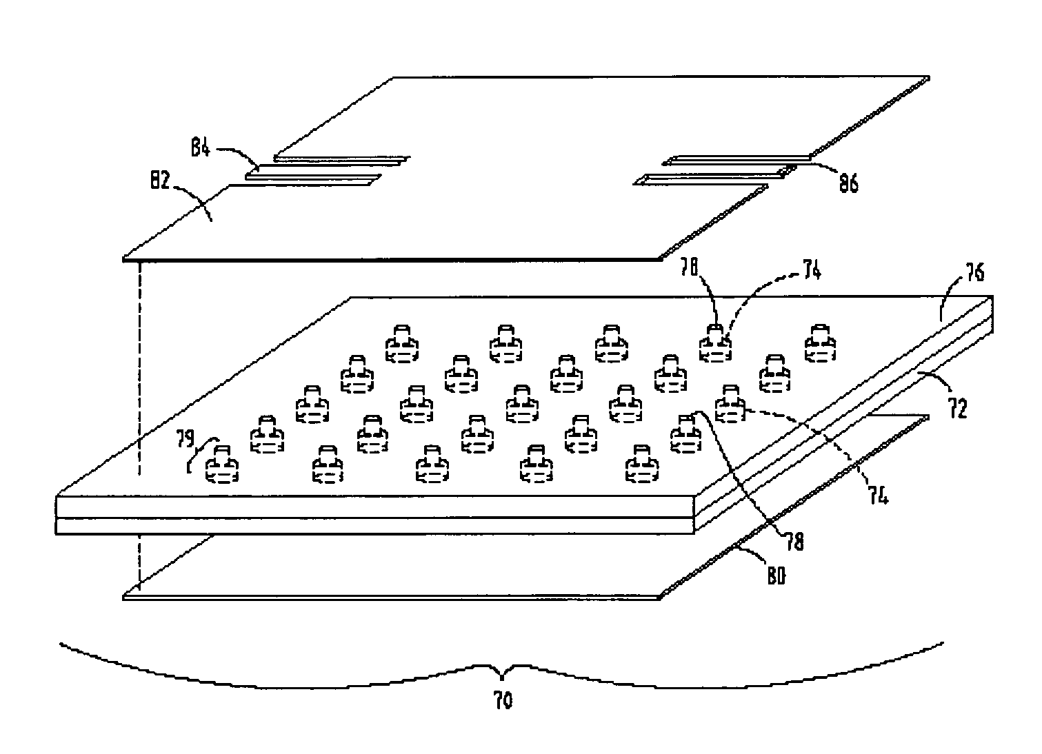
[0021]Referring to FIG. 2, an Electromagnetic Bandgap (EBG) device 70 is shown including a first planar substrate 72. As shown, first planar substrate 72 includes a periodic lattice of vias 74 embedded in first planar substrate 72. In the present embodiment, first planar substrate 72 is made of low-temperature co-fired ceramic (LTCC), and the periodic lattice of vias 74 are conductive vias formed in the shape of columns or rods. First planar substrate 72 has a lower surface and an upper surface, and conductive vias 74, formed in first planar substrate 72, extend from the lower surface of first planar substrate 72 to the upper surface of first planar substrate 72. More specifically, lower surfaces of the conducting vias 74 are exposed on the lower surface of first planar substrate 72, and upper surfaces of conductive vias 74 are exposed on the upper surface of first planar substrate 72. As shown, the conductive vias 74 are in the form of cylindrical columns that have a height equal t...


PUM

PropertyMeasurementUnit
bandgap frequencyaaaaaaaaaa
resonant frequencyaaaaaaaaaa
band gap frequencyaaaaaaaaaa

Abstract

A high-frequency Electromagnetic Bandgap (EBG) device, and a method for making the device are provided. The device includes a first substrate including multiple conducting vias forming a periodic lattice. The vias of the first substrate extend from the lower surface of the first substrate to the upper surface of the first substrate. The device also includes a second substrate having multiple conducting vias forming a periodic lattice. The vias of the second substrate extend from the lower surface of the second substrate to the upper surface of the second substrate. The second substrate is positioned adjacent to, and overlapping, the first substrate, such that the lower surface of the second substrate is in contact with the upper surface of the first substrate, and such that a plurality of vias of the second substrate are in contact with a corresponding plurality of vias of the first substrate.

Description

TECHNICAL FIELD[0001]The present invention generally relates to Electromagnetic Bandgap (EBG) devices, and more particularly, to EBG devices having high bandgap and resonant frequencies.BACKGROUND OF THE INVENTION[0002]EBG devices are devices generally having an ability to suppress and filter electromagnetic energy. EBG devices are often used to help suppress switching noise and electromagnetic radiation in printed circuit boards (PCBs) and packages containing electronic devices. Such devices are also sometimes used to improve the performance of planar antennas by reducing cross-coupling between antenna array elements through surface waves, and by suppressing and directing radiation. EBG devices can be useful in other active and passive devices and applications such as oscillators, waveguides, transmission lines, amplifiers, filters, power combining circuits, phased arrays, mixers, and microwave components and devices.[0003]A typical EBG device generally has a periodic structure, su...

Claims


Application Information

Patent Timeline
Patent Type & Authority Patents(United States)
IPC IPC(8): H01Q1/38H01Q15/02
CPCH01P1/2005H05K1/0216H01Q15/0026H01Q15/006H05K2201/09309Y10T29/49016H05K2201/09609
Inventor BERLIN, CARL W.NAIR, DEEPUKUMAR M.
Owner APTIV TECH LTD
Why Eureka
Try Eureka