Drive circuit and drive method for panel display device

a technology of drive circuit and display device, which is applied in the direction of static indicating devices, instruments, electroluminescent light sources, etc., can solve the problems of uneven display and deteriorated emission intensities, and achieve the effect of increasing charging speed and speed

Inactive Publication Date: 2009-09-08
LAPIS SEMICON CO LTD
View PDF9 Cites 2 Cited by
  • Summary
  • Abstract
  • Description
  • Claims
  • Application Information

AI Technical Summary

Benefits of technology

[0012]The drive circuit for a panel display device and the drive method for a panel display device according to the present invention accelerate the rise for charging up to the voltage necessary for light emission, thus enabling to charge at higher speed.

Problems solved by technology

The rise time required for charging up to a voltage necessary for light emission is long, thus causing such problems as deteriorated emission intensities of the organic EL devices PEP,Q and uneven display (variations in brightness).

Method used


Image

  • Drive circuit and drive method for panel display device
  • Drive circuit and drive method for panel display device
  • Drive circuit and drive method for panel display device

Examples


first embodiment

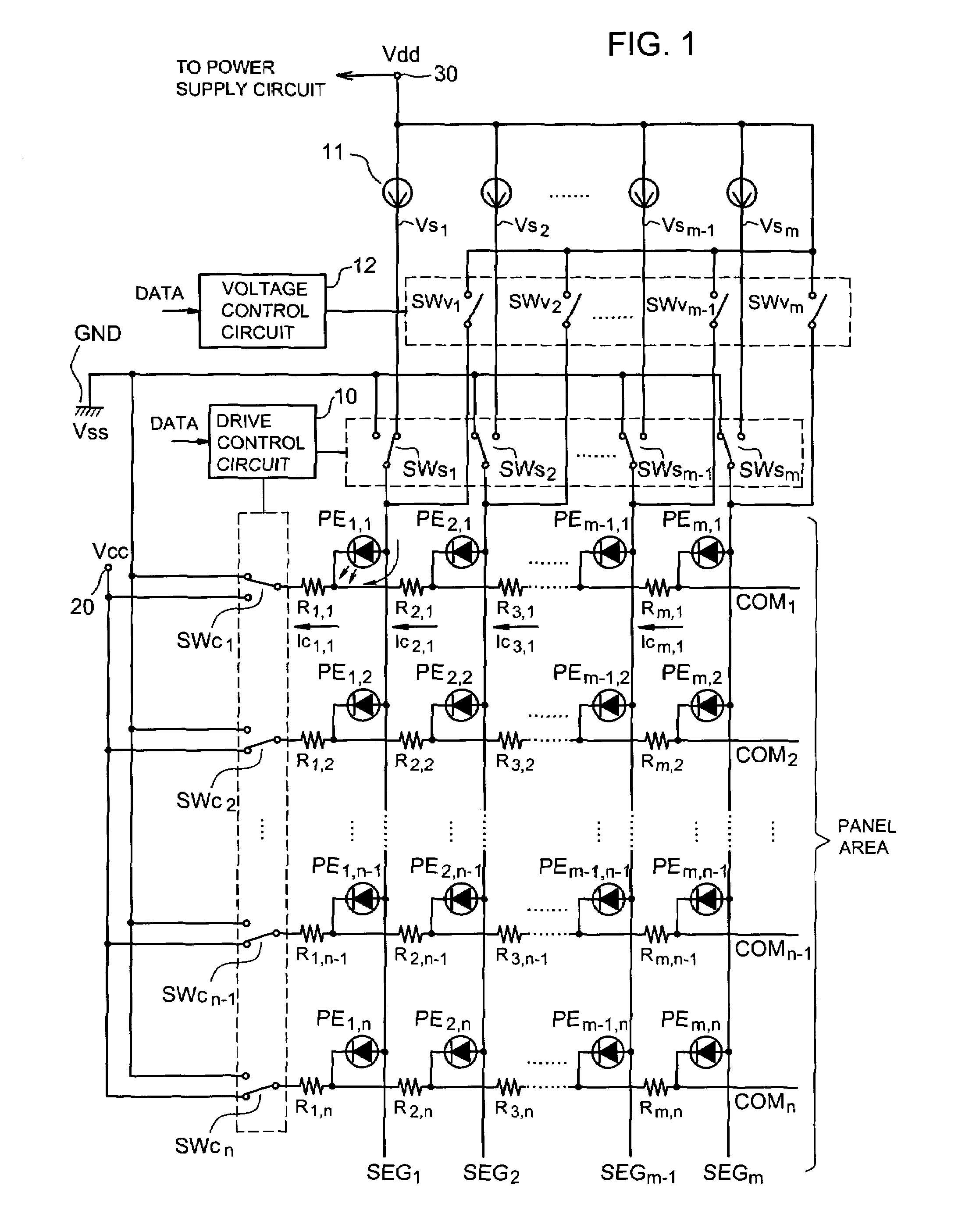
[0020]FIG. 1 is a block diagram illustrating a drive circuit for a panel display device which is the present invention. The organic EL panel display device has light-emitting devices, or organic EL devices PEP,Q (P is an integer ranging from 1 to n; Q is an integer ranging from 1 to m), which are arranged at respective intersections between a plurality of data lines (anode lines) SEG1 to SEGm and a plurality of scan lines (cathode lines) COM1 to COMn (m and n are integers no smaller than 2).

[0021]The drive circuit for the panel display device according to the present invention comprises first switch circuits SWsP, second switch circuits SWcQ, and third switch circuits SWvP. The first switch circuits SWsP connect the data lines SEGP to either respective constant current sources 11 or a ground potential Vss. The second switch circuits SWcQ connect the respective scan lines COMQ to either one of a scan line power supply 20 (power supply potential Vcc) and the ground voltage Vss. The th...

second embodiment

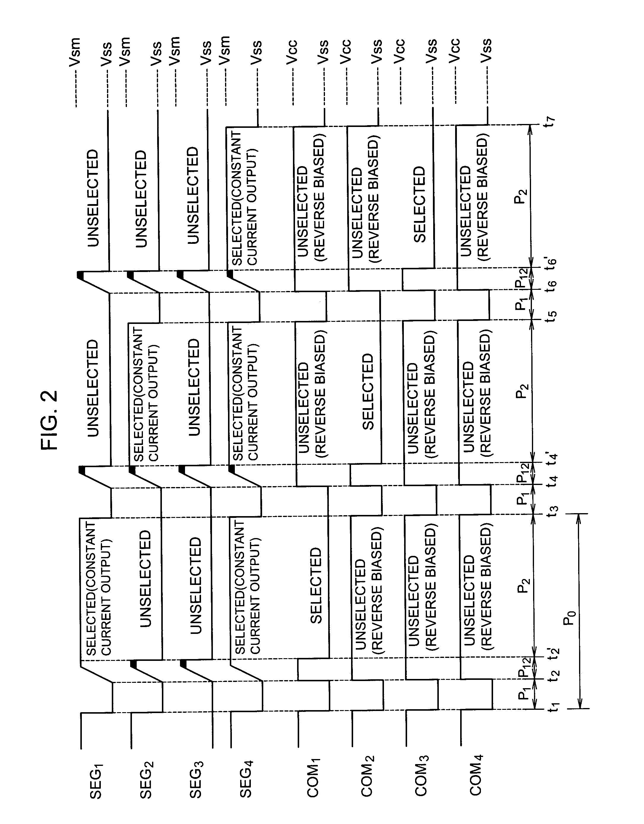
[0031]Next, with reference to the timing chart shown in FIG. 8, description will be given of the operation of driving a panel display device which is the present invention.

[0032]Here, the drive circuit for the panel display device may be configured the same as in the first embodiment of the present invention.

[0033]In the period P1, the switch circuits SWsP are turned OFF as shown in FIG. 4. The switch circuit SWc1 is connected to the power supply potential Vcc. Then, the voltage control circuit 12 turns ON the switch circuits SWvP to charge the loads of the organic EL devices PEP,Q up to a certain potential (target potential Vsm). Consequently, discharging is achieved in H level.

[0034]Subsequently, in the period P2, as shown in FIG. 5, the voltage control circuit 12 turns OFF the switch circuits SWvP, so that the potentials of the data lines SEGP are kept at a certain potential (Vsm±α; α is arbitrary). At time t4, as shown in FIG. 6, the switch circuit SWs2 is connected to the const...


PUM


Abstract

Disclosed is a drive circuit for a panel display device for driving light-emitting devices arranged at respective intersections between a plurality of data lines and a plurality of scan lines. This drive circuit includes a voltage control circuit for charging the light-emitting devices to a voltage necessary for light emission by connecting the data lines to a predetermined power supply potential in a rising period prior to a period for selectively causing the light-emitting devices to emit light; and a drive control circuit for selectively connecting the data lines to a constant current source after the rising period.

Description

BACKGROUND OF THE INVENTION[0001]1. Field of the Invention[0002]The present invention relates to a drive circuit and a drive method for a panel display device, and particularly to a drive circuit and a drive method for a panel display device which are capable of charging light-emitting devices at high speed.[0003]2. Description of the Related Art[0004]FIG. 9 illustrates an organic EL panel display device which has organic EL devices PEP,Q (P is an integer ranging from 1 to m; Q is an integer ranging from 1 to n) arranged at respective intersections between a plurality of data lines (anode lines) SEG1 to SEGm (m is an integer no smaller than 2) and a plurality of scan lines (cathode lines) COM1 to COMn (n is an integer no smaller than 2). A drive device of this organic EL panel display device has switch circuits SWs1 to SWsm for connecting the data lines SEGP to respective constant current sources 11, and switch circuits SWc1 to SWcn for connecting the respective scan lines COMQ to a...

Claims


Application Information

Patent Timeline
Patent Type & Authority Patents(United States)
IPC IPC(8): G09G3/32H05B44/00
CPCG09G3/3216G09G3/3266G09G3/3283G09G2320/0223G09G2310/0256G09G2310/063G09G2310/08G09G2310/0251G09G3/30
Inventor SATOH, SHINICHIKIMURA, NAOYAHARA, TETSURO
Owner LAPIS SEMICON CO LTD
Why Eureka
Try Eureka