Semiconductor device and manufacturing method thereof

a semiconductor device and semiconductor technology, applied in semiconductor devices, semiconductor/solid-state device details, electrical equipment, etc., can solve the problems of inability to meet the future expectation of improved operation speed of the semiconductor device, limit the transmission speed of electric signals, etc., to achieve high speed and improve signal propagation speed

Inactive Publication Date: 2009-09-29
TESSERA ADVANCED TECH
View PDF25 Cites 65 Cited by
  • Summary
  • Abstract
  • Description
  • Claims
  • Application Information

AI Technical Summary

Benefits of technology

[0009]In view of the above problems, it is an object of the present invention to implement a high-density, high-performance semiconductor device capable of transmitting a signal with an external equipment at a high speed by improving a signal propagation speed between chips in a semiconductor device having two or more semiconductor chips stacked on each other.

Problems solved by technology

This puts limitations on improvement in transmission speed of electric signals.
Therefore, such a conventional semiconductor device cannot meet future expectation of improved operation speed of the semiconductor device.

Method used


Image

  • Semiconductor device and manufacturing method thereof
  • Semiconductor device and manufacturing method thereof
  • Semiconductor device and manufacturing method thereof

Examples


first embodiment

[0041]Hereinafter, a semiconductor device according to the first embodiment of the present invention and a manufacturing method thereof will be described.

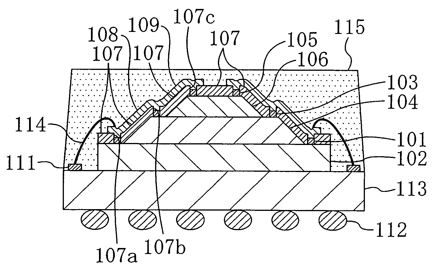
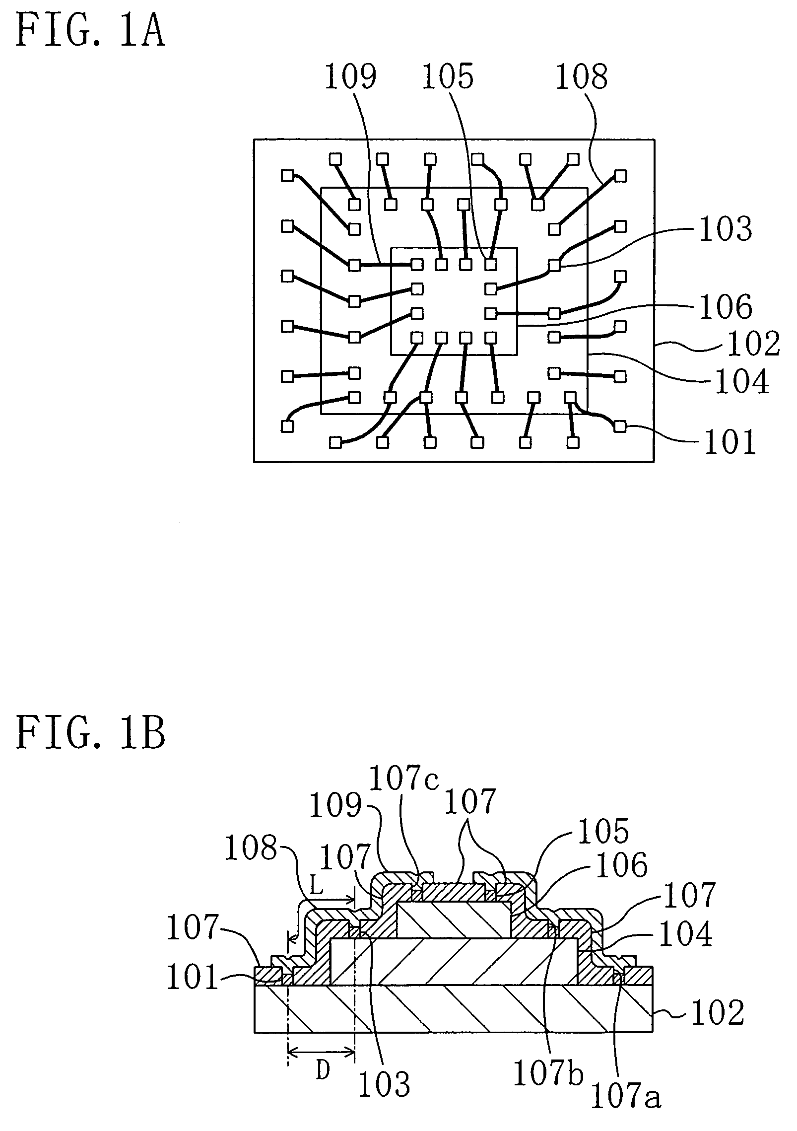
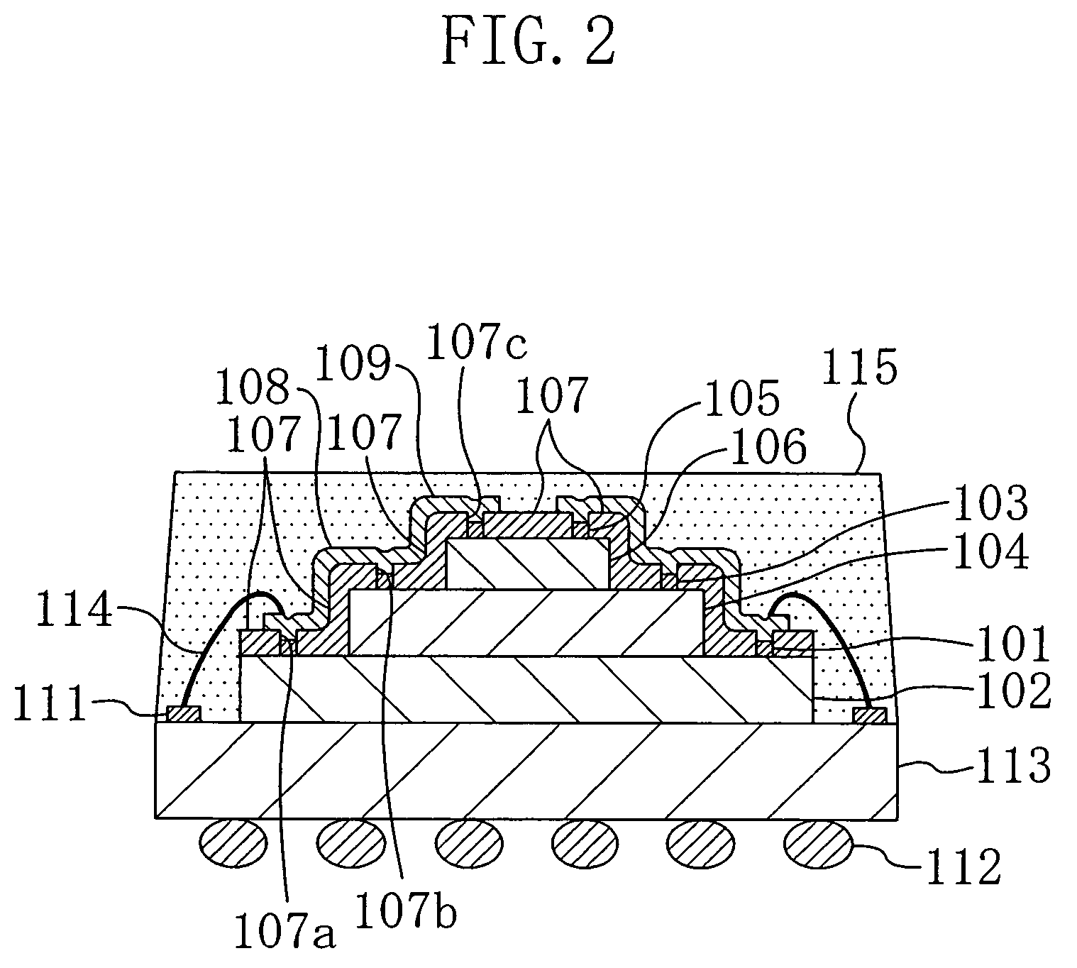
[0042]First, the structure of a stacked-chip element mounted in a single package in a semiconductor device of the first embodiment (hereinafter, referred to as “stacked-chip element of the present embodiment”) will be described with reference to the accompanying drawings. FIG. 1A is a plan view of the stacked-chip element of the present embodiment, and FIG. 1B is a cross-sectional view of an electrode portion of the stacked-chip element of the present embodiment.

[0043]Referring to FIGS. 1A, 1B, the stacked-chip element of the present embodiment includes a first semiconductor chip 102, a second semiconductor chip 104 and a third semiconductor chip 106. The first semiconductor chip 102 has first electrodes 101 on the fringe region of its main surface. The second semiconductor chip 104 is smaller in area than the first semiconductor c...

second embodiment

[0067]Hereinafter, a semiconductor device according to the second embodiment of the present invention and a manufacturing method thereof will be described.

[0068]First, the structure of a stacked-chip element mounted in a single package in the semiconductor device of the second embodiment (hereinafter, referred to as “stacked-chip element of the present embodiment”) will be described with reference to the accompanying drawings. FIG. 5A is a plan view of the stacked-chip element of the present embodiment. FIG. 5B is a cross-sectional view of an electrode portion of the stacked-chip element of the present embodiment. Note that, in FIGS. 5A, 5B, the same members as those of the stacked-chip element mounted in the semiconductor device of the first embodiment in FIGS. 1A, 1B are denoted with the same reference numerals and characters, and description thereof will be omitted.

[0069]As shown in FIGS. 5A, 5B, the stacked-chip element of the present embodiment is different from that of the fir...


PUM


Abstract

The semiconductor device includes a first semiconductor chip having first electrodes on a fringe region of a main surface thereof, and a second semiconductor chip smaller in area than the first semiconductor chip and having second electrodes on a main surface thereof. The first semiconductor chip and the second semiconductor chip are connected together by bonding a surface of the second semiconductor chip that is opposite to the main surface thereof to a region of the main surface of the first semiconductor chip other than the fringe region. The first electrodes are connected to the second electrodes by wirings formed over the main surface of the first semiconductor chip, a side surface of the second semiconductor chip and the main surface of the second semiconductor chip.

Description

RELATED APPLICATION[0001]This application is a divisional of application Ser. No. 10 / 185,000 filed Jul. 1, 2002 now abandoned.BACKGROUND OF THE INVENTION[0002]The present invention generally relates to a stacked-chip semiconductor device in which a plurality of semiconductor chips having different functions are stacked in a three-dimensional direction, and a manufacturing method thereof. More particularly, the present invention relates to a stacked-chip semiconductor device adapted for improved transmission speed of electric signals, and a manufacturing method thereof.[0003]Recently, a stacked-chip semiconductor device is developed in which a plurality of semiconductor chips having different functions are stacked on a single circuit board (carrier substrate) in a single package.[0004]Hereinafter, a semiconductor device having three semiconductor chips stacked on a circuit board will be described as a typical example of such a conventional stacked-chip semiconductor device.[0005]FIG....

Claims


Application Information

Patent Timeline
Patent Type & Authority Patents(United States)
IPC IPC(8): H01L21/00H01L21/60H01L23/31H01L25/065H01L29/06
CPCH01L29/0657H01L23/3128H01L24/24H01L24/82H01L24/91H01L24/94H01L25/0657H01L2224/16145H01L2924/07802H01L2224/82007H01L2924/01033H01L2224/24011H01L2224/24145H01L2224/24226H01L2224/24998H01L2224/32145H01L2224/48091H01L2224/48145H01L2224/48227H01L2225/06524H01L2225/06555H01L2225/06582H01L2924/01029H01L2924/01078H01L2924/01082H01L2924/10157H01L2924/15311H01L24/48H01L2924/00014H01L2924/00H01L24/45H01L2224/05554H01L2224/451H01L2924/10161H01L2924/10162H01L2924/181H01L2924/00015H01L2224/05599H01L2924/00012
Inventor SHIMOISHIZAKA, NOZOMIFUKUDA, TOSHIYUKI
Owner TESSERA ADVANCED TECH
Why Eureka
Try Eureka