High-frequency switching circuit, high-frequency module, and wireless communications device

a high-frequency switching and high-frequency module technology, applied in the field of high-frequency switching circuits, high-frequency modules, wireless communications devices, can solve the problems of passing power loss, inability to meet the request for downsizing, etc., and achieve the effect of shortening the design and manufacturing lead-time and reducing costs

Inactive Publication Date: 2009-09-29
KYOCERA CORP
View PDF4 Cites 139 Cited by
  • Summary
  • Abstract
  • Description
  • Claims
  • Application Information

AI Technical Summary

Benefits of technology

[0020]Accordingly, it is an object of the present invention to provide a high-frequency switching circuit capable of reducing cost by eliminating the need for designing and manufacturing many kinds of different high-frequency switches and further shortening the designing and manufacturing lead-time for such high-frequency switches or high-frequency switching circuits using the high-frequency switches.
[0021]It is also an object of the present invention to provide a high-frequency switching circuit capable of reducing passing loss in the path between a common antenna terminal and a high-frequency switch and of ensuring a large amount of attenuation.
[0022]It is a further object of the present invention to provide a low-cost high-frequency module and wireless communications device including a high-frequency switching circuit that supports many bands.

Problems solved by technology

Therefore, there occurs a problem in that the above-described request for downsizing cannot be met.
Inserting the demultiplexing circuit DIPX1 also suffers from another problem in that there occurs a passing loss of power between the common antenna terminal and the common terminal of each high-frequency switch in both transmission and reception systems.
This requires many kinds of high-frequency switches to be designed and manufactured, resulting in many disadvantages.

Method used


Image

  • High-frequency switching circuit, high-frequency module, and wireless communications device
  • High-frequency switching circuit, high-frequency module, and wireless communications device
  • High-frequency switching circuit, high-frequency module, and wireless communications device

Examples


Embodiment Construction

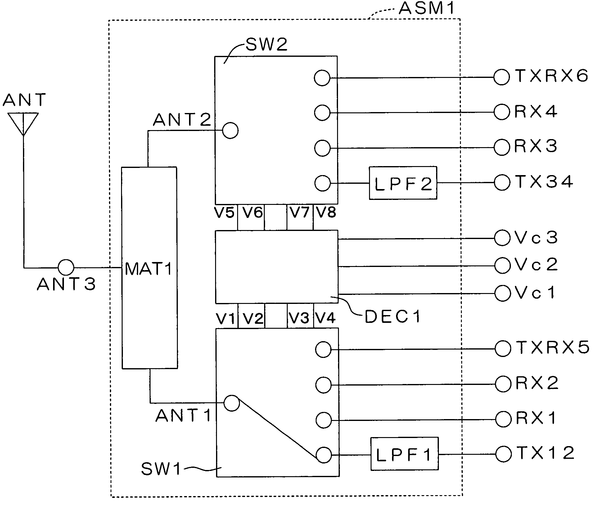
FIG. 1 is a block diagram illustrating an example of a high-frequency switching circuit of a multiband-compliant mobile phone unit according to the present invention.

[0073]The high-frequency switching circuit ASM1 is connected to a common antenna terminal ANT3 and is adapted to switch among six communication systems of GSM850 (850 MHz band), GSM900 (900 MHz band), DCS (1800 MHz band), PCS (1900 MHz band), CDMA Cellular (800 MHz band), and UMTS (2100 MHz band).

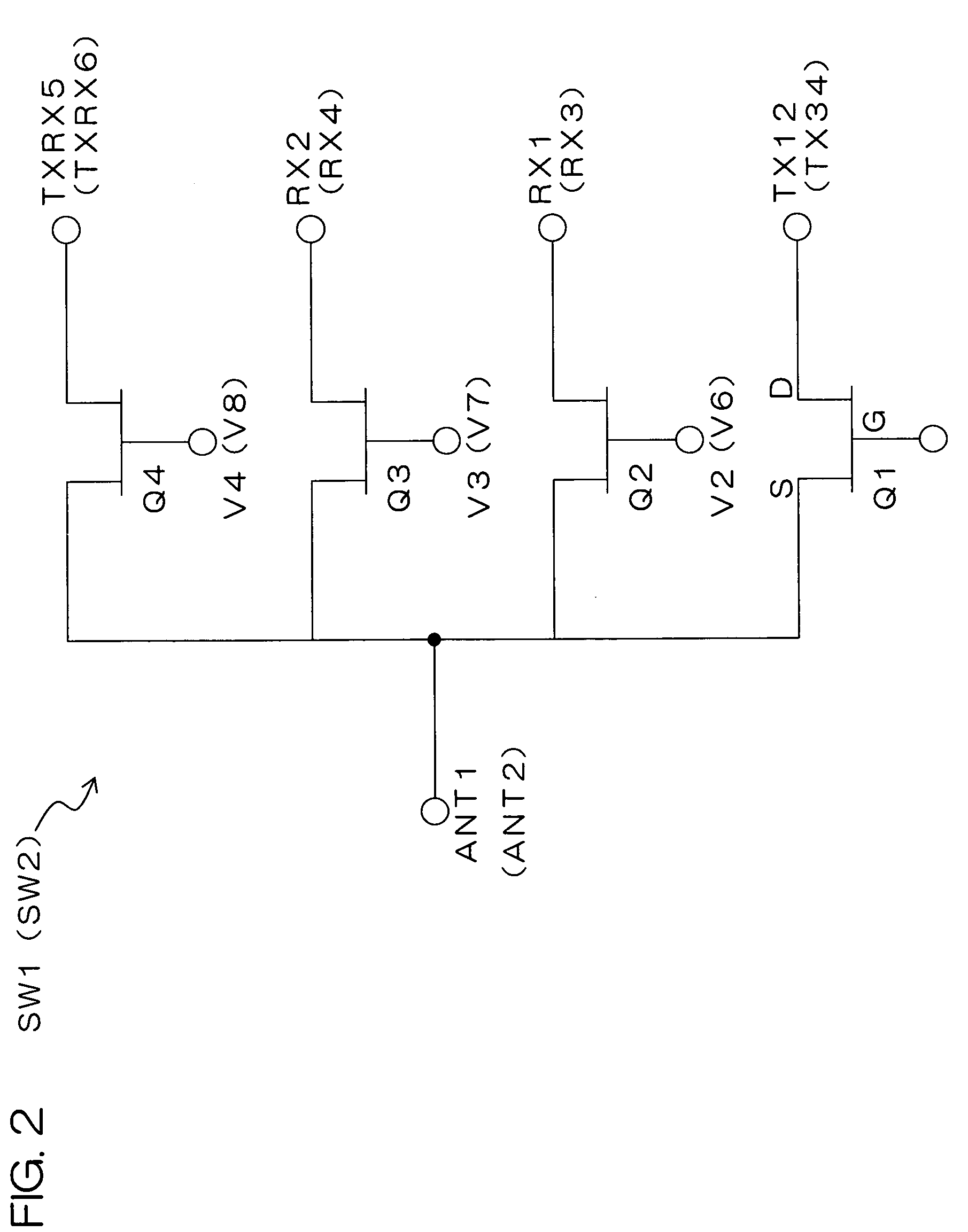
[0074]The high-frequency switching circuit ASM1 comprises a high-frequency switch SW1 adapted to switch among TX12 (GSM850 / 900-TX), RX1 (GSM850-RX), RX2 (GSM900-RX), and TXRX5 (CDMACellular-TX / RX), and a high-frequency switch SW2 adapted to switch among TX34 (DCS / PCS-TX), RX3 (DCS-RX), RX4 (PCS-RX), and TXRX6 (UMTS-TX / RX).

[0075]Both an antenna side terminal ANT1 of the high-frequency switch SW1 and an antenna side terminal ANT2 of the high-frequency switch SW2 are connected to the common antenna terminal ANT3 via an impedance m...


PUM


Abstract

The present invention provides a high-frequency switching circuit comprising: two or more high-frequency switches SW1 and SW2 provided correspondingly to a plurality of communication systems having mutually different frequency bands; and a control circuit DEC1 adapted to control the switching of the two or more high-frequency switches SW1 and SW2, in which a common antenna terminal ANT3 and common terminals ANT1 and ANT2 of the respective high-frequency switches SW1 and SW2 are connected via a matching circuit MAT1 having a filtering function capable of allowing passage of direct current. When one path of the high-frequency switch SW1 is turned on, the other paths of the high-frequency switch SW1 and all paths of the high-frequency switch SW2 can be turned off.

Description

BACKGROUND OF THE INVENTION[0001]1. Field of the Invention[0002]The present invention relates to a high-frequency switching circuit, a high-frequency module including the high-frequency switching circuit, and a wireless communications device mounted with the high-frequency module, which are used particular in a multiband-compliant mobile radio terminal preferably.[0003]2. Description of Related Art[0004]In recent years, there have been proposed mobile phones employing a multiband system, mounted with two or more communication systems in a single mobile phone. Multiband mobile phones, which can perform transmission / reception by selecting a communication system suitable for regional characteristics, intended use, etc., are expected to be convenient ones. For example, there exist dual-band mobile phones that have two communication systems of GSM (Global System for Mobile Communication) and DCS (Digital Cellular System) as a plurality of communication systems having mutually different c...

Claims


Application Information

Patent Timeline
Patent Type & Authority Patents(United States)
IPC IPC(8): H04B1/44H03H11/34H04B1/40H04B1/50H04Q7/20
CPCH04B1/006H04B1/0057
Inventor NAKAMATA, KATSURONINOMIYA, HIROSHIHORIUCHI, MASAFUMIISOYAMA, SHINJITAKAHASHI, TOORU
Owner KYOCERA CORP
Why Eureka
Try Eureka