Liquid crystal display device and electronic apparatus
a display device and liquid crystal technology, applied in closed circuit television systems, instruments, television systems, etc., can solve the problems of deviation in thickness of retardation or disturbance in alignment of liquid crystal polymers constituting retardation layers, difficulty in obtaining high contrast, and narrow viewing angle at the time of transmissive display. achieve high contrast, wide viewing angle, and high contrast
- Summary
- Abstract
- Description
- Claims
- Application Information
AI Technical Summary
Benefits of technology
Problems solved by technology
Method used
Image
Examples
first embodiment
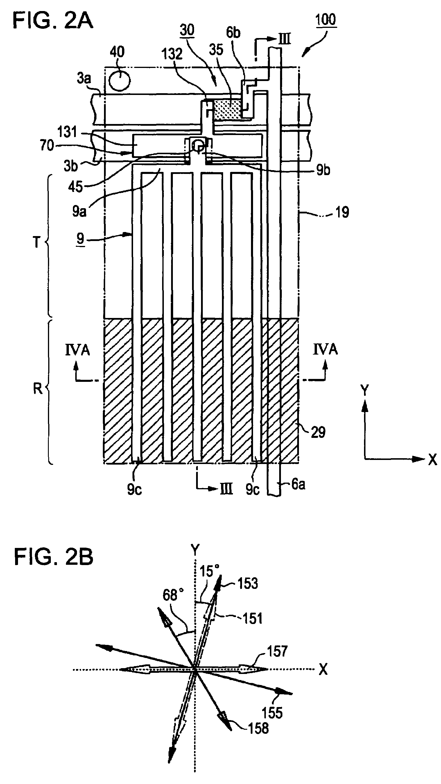
[0039]Hereinafter, a liquid crystal display device according to a first embodiment of the present invention will be described with reference to the drawings. The liquid crystal display device according to the first embodiment employs a fringe field switching (FFS) mode among transverse electric field modes which display an image by applying an electric field (transverse electric field) to liquid crystal molecules in a in-plane direction of a substrate to control alignment of the liquid crystal molecules.
[0040]The liquid crystal display device according to the first embodiment a color liquid crystal display device having a color filter on the substrate, in which three sub pixels emitting colored light components of red (R), green (G), and blue (B) form a pixel. Accordingly, a display area serving as a unit constituting display is referred to as a “sub pixel area” and a display area including a set of sub pixels (R, G, and B) is referred to as a “pixel area.”
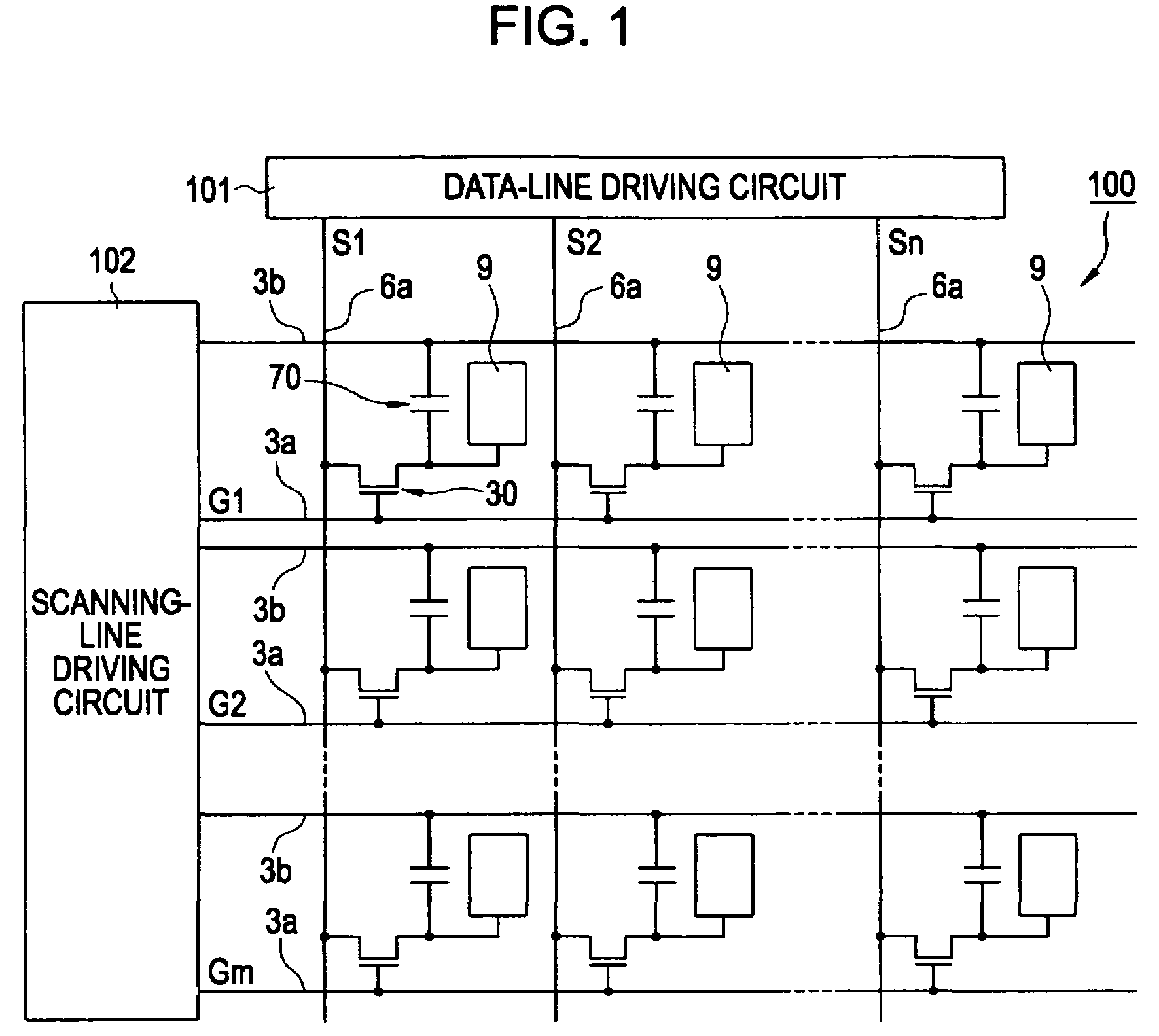
[0041]FIG. 1 is a circuit ...
second embodiment
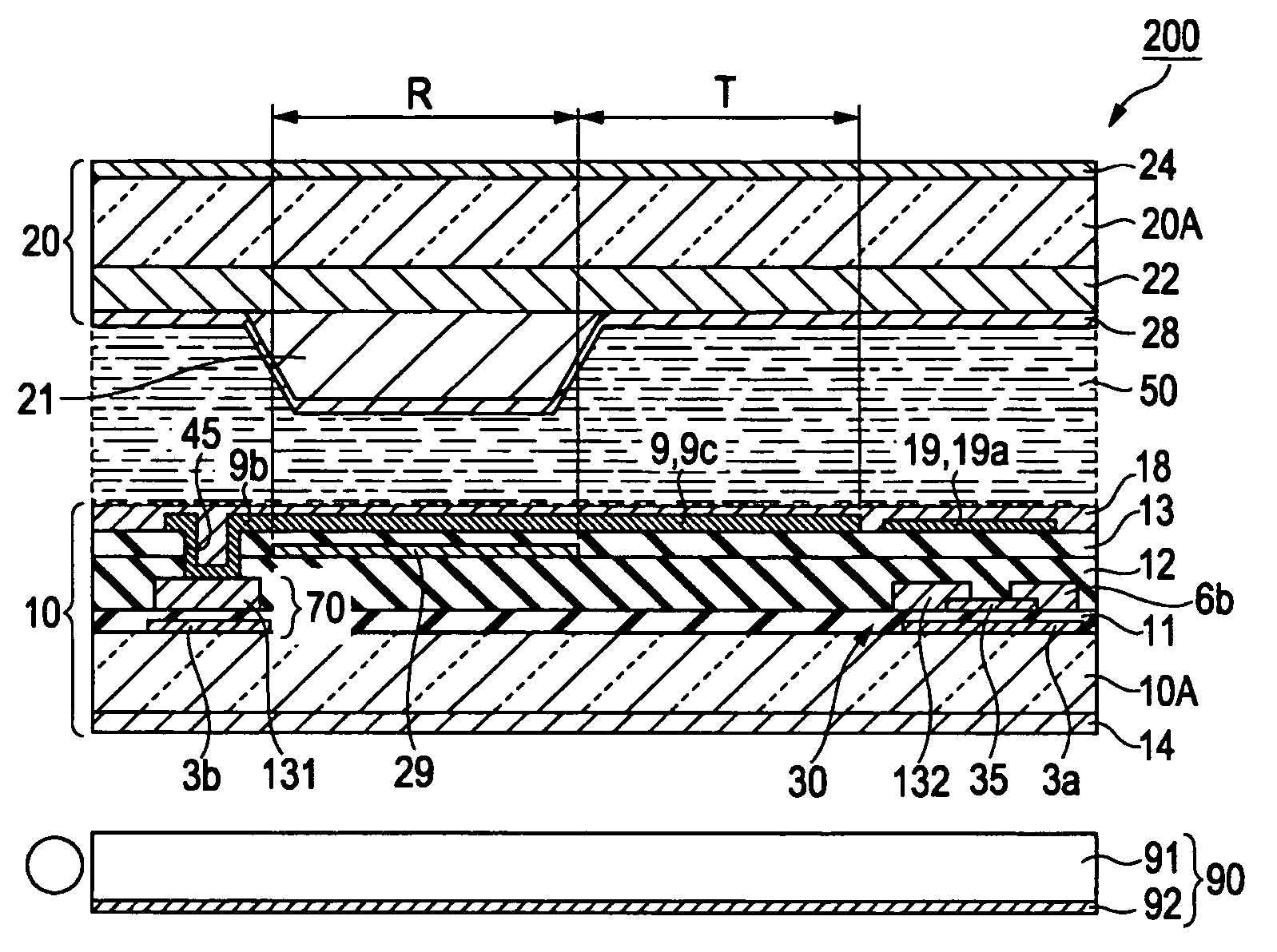
[0075]Next, a second embodiment of the invention will be described with reference to the drawings. FIG. 5A is a plan view illustrating a sub pixel area of a liquid crystal display device 200 and FIG. 5B is a diagram illustrating arrangement of optical axes in FIG. 5A. FIG. 6 is a partially sectional view taken along Line D-D′ of FIG. 5A.
[0076]The liquid crystal display device 200 according to the second embodiment has a basic structure substantially similar to that of the liquid crystal display device 100 according to the first embodiment, but is different from the liquid crystal display device 100 in that the pixel electrode 9 and the common electrode 19 are both formed in a pectinated shape as seen two-dimensionally, and band-shaped electrodes (branched electrodes) constituting the pectinated portions and extending in a rod shape are formed in the same layer. In addition, in FIGS. 5, 6, and 7, the same reference numerals denote the same elements as the liquid crystal display devic...
third embodiment
[0104]Next, a third embodiment of the invention will be described with reference to FIG. 8. A liquid crystal display device 300 according to the third embodiment has the same basic structure as the liquid crystal display device according to the first embodiment, but is different from the liquid crystal display device according to the first embodiment, in that a resin layer 23 and a retardation layer 21 are stacked in an area on the color filter 22 corresponding to the reflective display area R. Accordingly, the two-dimensional structure of a sub pixel area and the arrangement of optical axes are completely equal to those of the first embodiment and thus description thereof is omitted. In FIG. 8, the same elements as the liquid crystal display device 100 shown in FIGS. 1 to 4 are denoted by the same reference numerals and detailed description thereof is omitted.
[0105]FIG. 8 is a partially sectional view illustrating the liquid crystal display device according to the third embodiment....
PUM
| Property | Measurement | Unit |
|---|---|---|
| thickness d1 | aaaaa | aaaaa |
| thickness d1 | aaaaa | aaaaa |
| thickness d1 | aaaaa | aaaaa |
Abstract
Description
Claims
Application Information


