Probe microscope and measuring method using probe microscope

a technology of probe microscope and probe microscope, which is applied in the direction of material analysis using wave/particle radiation, instruments, nuclear engineering, etc., can solve the problems of many methods which can be applied, complicated measurement, and small number of methods which are practically used or widely used, and achieve the effect of accurately measuring the electronic state density

Inactive Publication Date: 2009-10-27
CANON KK
View PDF8 Cites 3 Cited by
  • Summary
  • Abstract
  • Description
  • Claims
  • Application Information

AI Technical Summary

Benefits of technology

[0045]The present invention has been made in view of the above-mentioned problems. An object of the present invention is to provide a probe microscope capable of accurately measuring an electronic state density of a surface of a high-resistance material, and a measuring method using the probe microscope.
[0050]According to the present invention, the electronic state density of the surface of the high-resistance material can be accurately measured. According to the present invention, the local measurement of the electronic state density of the surface of the high-resistance material which was conventionally difficult can be performed.

Problems solved by technology

However, the number of methods which are practically used or widely used is small.
Many methods can be applied to only a few materials, or require complicated measurement and take a very long time.
According to the above-mentioned evaluation method using the combination of the X-ray photoelectron spectroscopy (XPS) or the ultraviolet photoelectron spectroscopy (UPS) and the inverse photoelectron spectroscopy (IPES), it is necessary to measure the sample in a high-vacuum environment, and the sample is likely to be damaged or charged up.
In particular, the charge up causes dulling of a spectral shape or a peak shift, thereby significantly reducing reliability of data.
In addition, because a device structure itself contains a metal and an insulator, it is difficult to measure a local electronic state of the sample to be measured by the existing STM / STS.
Therefore, this measurement takes a very long time and it is difficult to measure an electronic state of a sample fixed at a certain point in the order of nanoscale or to form an image of a result obtained by the measurement.
However, a way to realize the method is not taken into account.

Method used


Image

  • Probe microscope and measuring method using probe microscope
  • Probe microscope and measuring method using probe microscope
  • Probe microscope and measuring method using probe microscope

Examples


example 1

[0129]In Example 1, a measuring method using the Kelvin probe force microscope based on the frequency shift detecting method will be described.

[0130]In this example, a probe device used for the probe microscope was formed as follows.

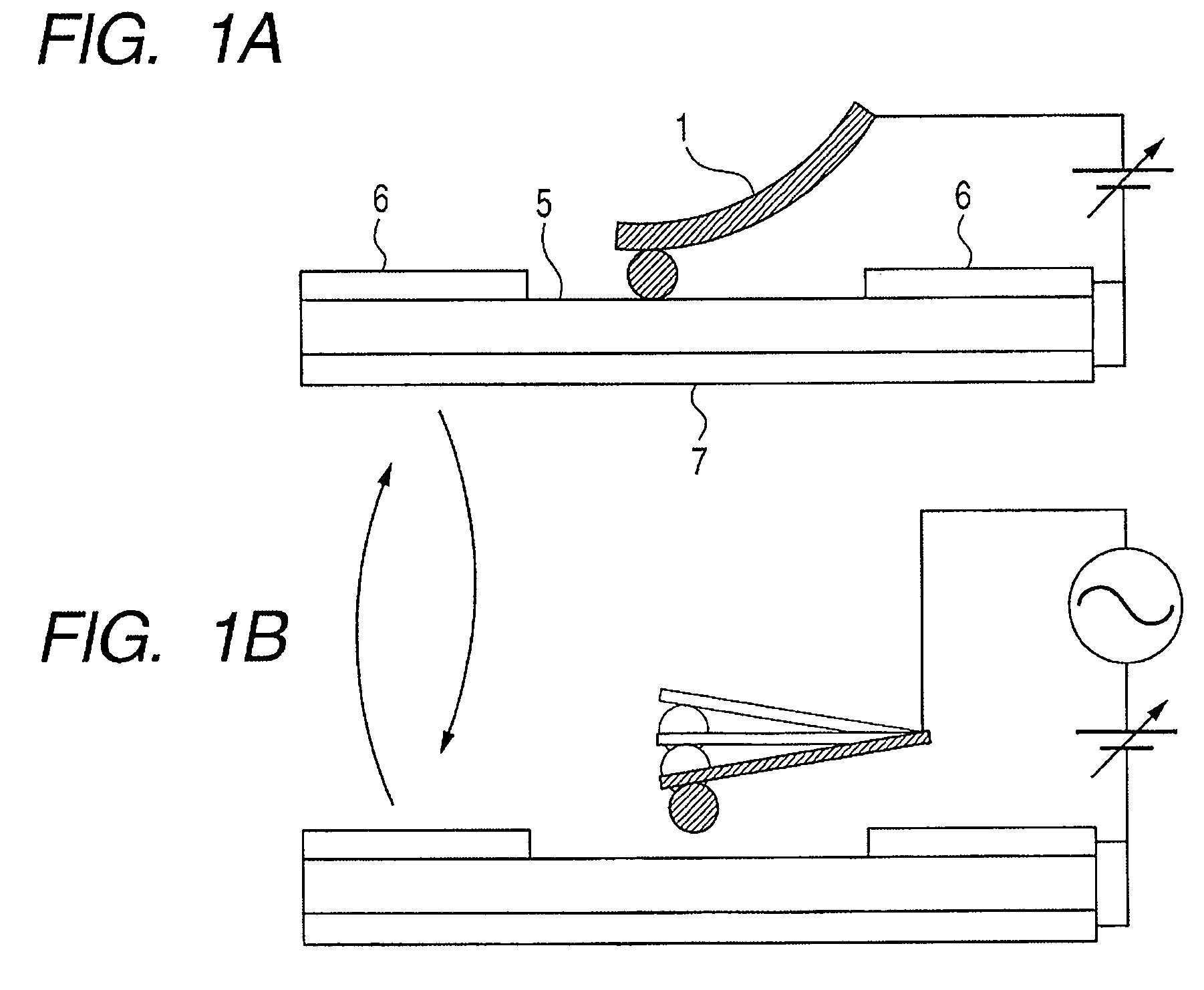
[0131]A commercially available cantilever for atomic force microscope without a probe (produced by NanoWorld AG, product name: TL-FM, spring constant: 3 N / m, resonance frequency: 75 kHz) was used as the cantilever.

[0132]A PMMA particle which was used for a probe device and had a diameter of 10 μm was bonded and fixed to the cantilever by a small amount of epoxy (produced by Gatan Inc., product name: G-1 Epoxy).

[0133]After that, a coating film which was made of Au and had a thickness of 50 nm was formed on the particle and each surface of the cantilever by a sputtering method.

[0134]Therefore, the probe device having the structure as illustrated in FIG. 2 was produced.

[0135]FIG. 6 is a schematic structural diagram illustrating a control circuit of the prob...

example 2

[0160]In Example 2, a measuring method using the Kelvin probe force microscope based on the amplitude shift detecting method will be described.

[0161]In this example, a probe device used for the probe microscope was the probe device having the same structure as that used in Example 1 as illustrated in FIG. 2.

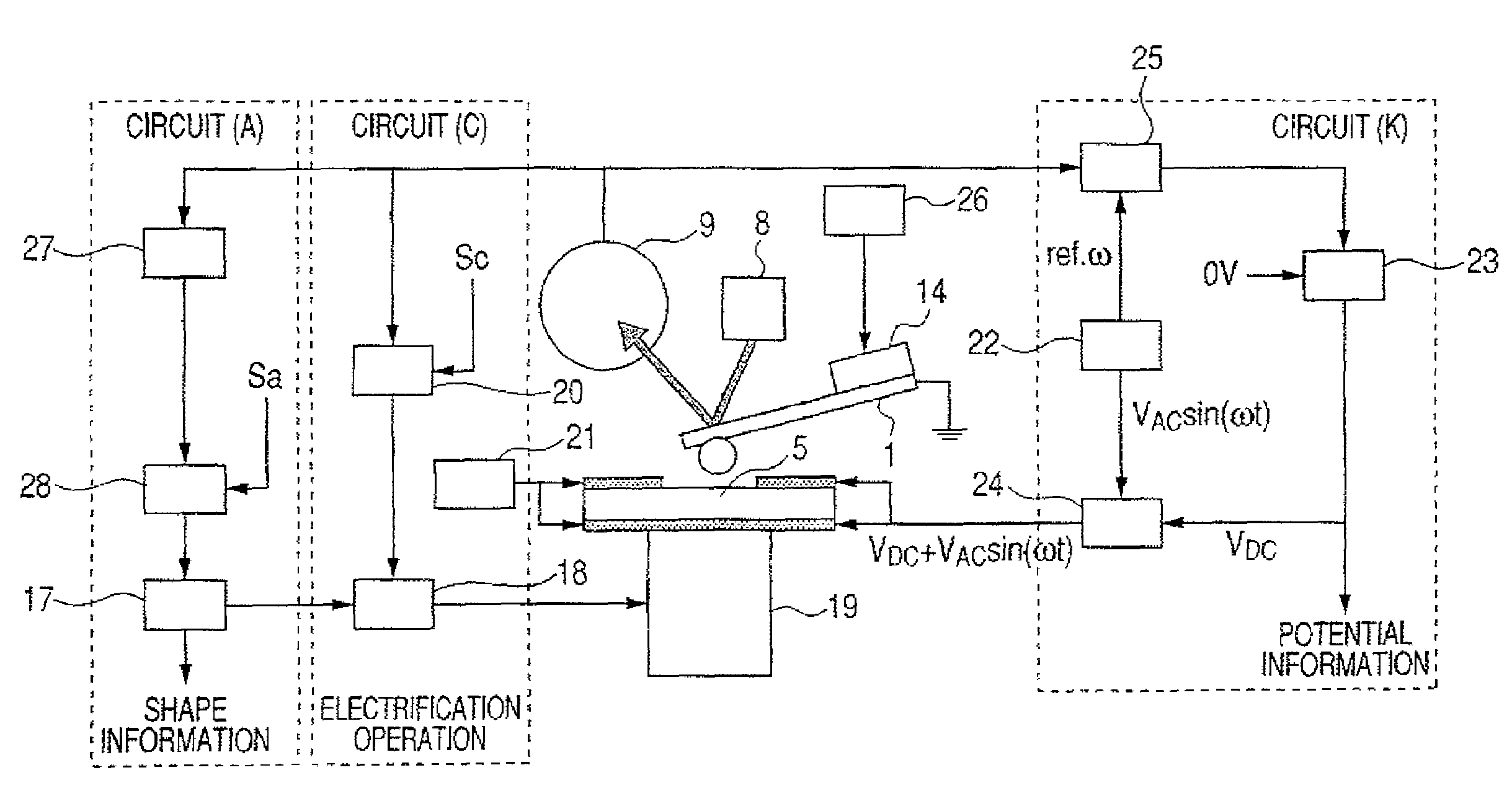
[0162]FIG. 7 is a schematic structural diagram illustrating a control circuit of the scanning probe microscope which is used in this example.

[0163]As illustrated in FIG. 7, the control circuit of a scanning probe microscope according to this example roughly includes four parts, that is, a circuit (C), a circuit (K), a circuit (A), and a normal control circuit other than the circuits.

[0164]The circuit (C) is used for electrification operation and includes a Z-piezoelectric driver 18, an error amplifier 20, and a DC power supply 21.

[0165]The circuit (K) is used for potential measurement and includes an oscillator 22, an error amplifier 23, an accumulator 24, and a lock-in amplifier...

example 3

[0186]In Example 3, a scanning probe microscope provided with the scanning function, which is configured to obtain an electronic state density distribution image, will be described.

[0187]The scanning probe microscope according to this example included the same control circuit as that in Example 1.

[0188]Therefore, when the in-plane scanning function of the scanning probe microscope is used, the measurement of the electronic state density as described in Example 1 can be sequentially performed while the position on the surface of the sample is changed. In view of the fact that each region of the surface of the sample is measured in this example, the measurement is based on the same idea as that in the current imaging tunneling spectroscopy (CITS) measurement in which I-V measurement is performed on each region of the surface of the sample.

[0189]However, according to the measuring method in this example, when the relationship between the applied voltage and the surface potential is to ...


PUM


Abstract

Provided is a probe microscope for measuring a surface potential of a sample, including a contact electrification mechanism (circuit (C)) for bringing an electroconductive probe device into contact with a surface of the sample and applying a voltage in the contact state to induce electrification on the surface of the sample, and a potential measuring mechanism (circuit (K)) for measuring the surface potential of the sample caused by the contact electrification mechanism in a non-contact state of the electroconductive probe device and the surface of the sample, wherein the electrification induced by the contact electrification mechanism and the measurement of the surface potential by the potential measuring mechanism alternate in time series while the voltage applied during the contact is gradually changed, thereby measuring a correlation between the applied voltage and the surface potential.

Description

BACKGROUND OF THE INVENTION[0001]1. Field of the Invention[0002]The present invention relates to a probe microscope and a measuring method using the probe microscope, more particularly, to a probe microscope capable of measuring an electronic state density of a surface of a high-resistance material, and a measuring method using the probe microscope.[0003]2. Description of the Related Art[0004]In recent years, a significant increase in performance of an electronic device represented by a silicon device and a reduction in size of the structure thereof have been realized, and an electronic device has been developed to achieve a structure size in an order of nanoscale.[0005]Not only an inorganic material but also an organic material and a polymer material are incorporated into the device as constituent materials.[0006]When the device becomes a nanoscale size, it is necessary to use a method of locally evaluating electronic characteristics of a portion which exerts a predetermined functi...

Claims


Application Information

Patent Timeline
Patent Type & Authority Patents(United States)
IPC IPC(8): G01R31/02G01Q70/12G01Q10/06G01Q30/04G01Q60/00G01Q60/24G01Q60/30G01Q60/40
CPCB82Y35/00G01Q60/30G01Q70/10G01Q60/40G01Q60/32
Inventor KUSAKA, TAKAO
Owner CANON KK
Why Eureka
Try Eureka