
Complementary metal oxide semiconductor image sensor having cross talk prevention and method for fabricating the same

a technology of metal oxide semiconductor and image sensor, which is applied in the direction of discharge tube/lamp details, instruments, discharge control devices, etc., can solve the problems of limited full factor, deterioration of cmos image sensor characteristics, and restrictions on effective avoidance of cross talk, so as to effectively minimize cross talk and effectively minimize cross talk

Inactive Publication Date: 2009-11-03
DONGBU ELECTRONICS CO LTD
View PDF17 Cites 29 Cited by
  • Summary
  • Abstract
  • Description
  • Claims
  • Application Information

AI Technical Summary

Benefits of technology

[0015]In considerations of the above problem, it is an aspect of the present invention to provide a CMOS image sensor for effectively minimizing cross talk. It is another aspect of the present invention to provide a method for fabricating a CMOS image sensor for effectively minimizing cross talk.
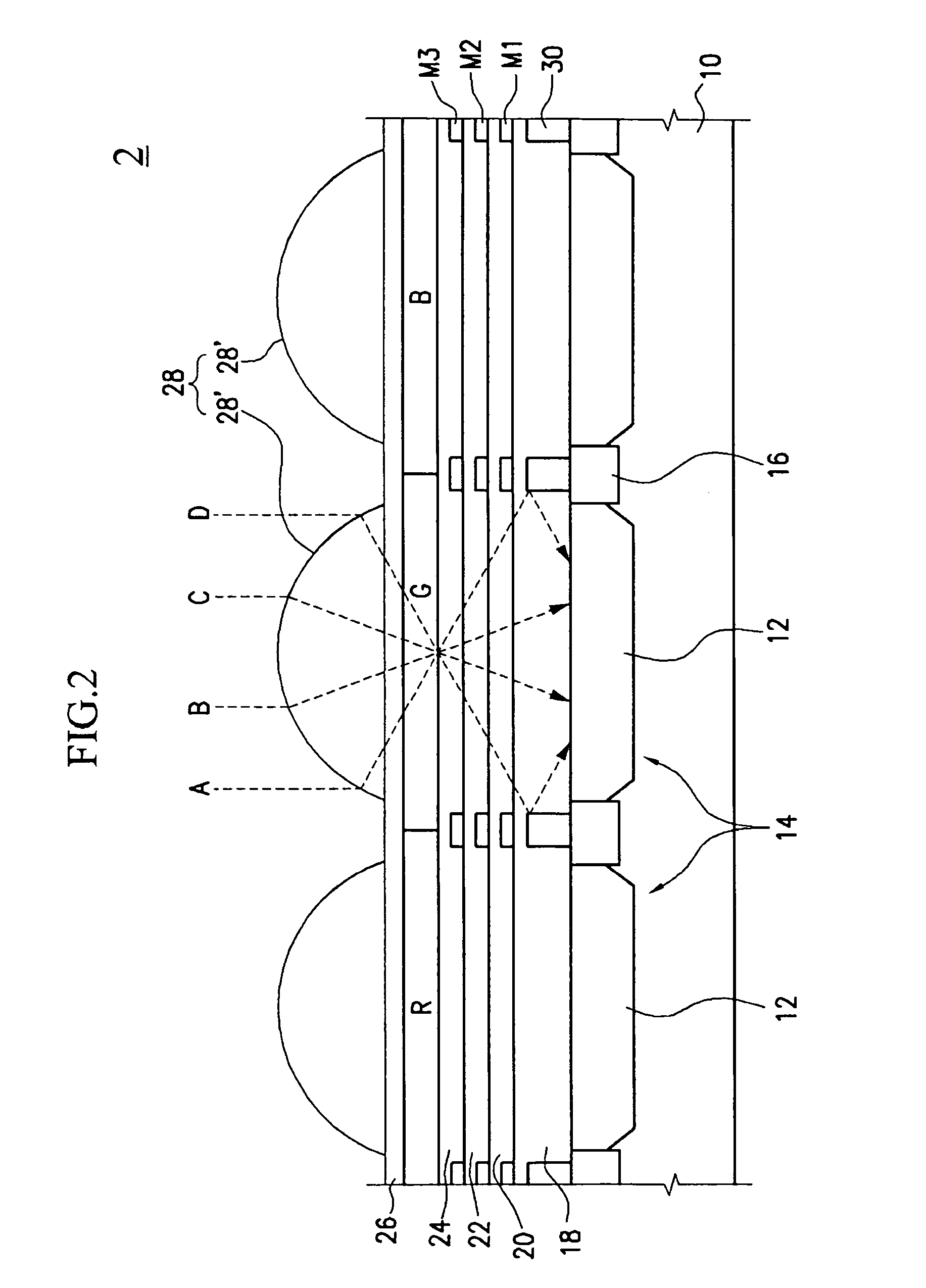
[0016]Consistent with the present invention, there is provided a CMOS image sensor including a semiconductor substrate; device isolation regions provided on the semiconductor for defining device regions therebetween; photocharge generating portions provided on the device regions for receiving external light and for generating and storing electric charges; light concentrating portions provided over the photocharge generating portions for concentrating the external light onto corresponding photocharge generating portions; and cross talk preventing portions for preventing the light passing through the light concentrating portions from being incident onto adjacent photocharge generating portions.

Problems solved by technology

However, the full factor is limited to the extent that the logic circuit also has to be formed within the area of the CMOS image sensor.
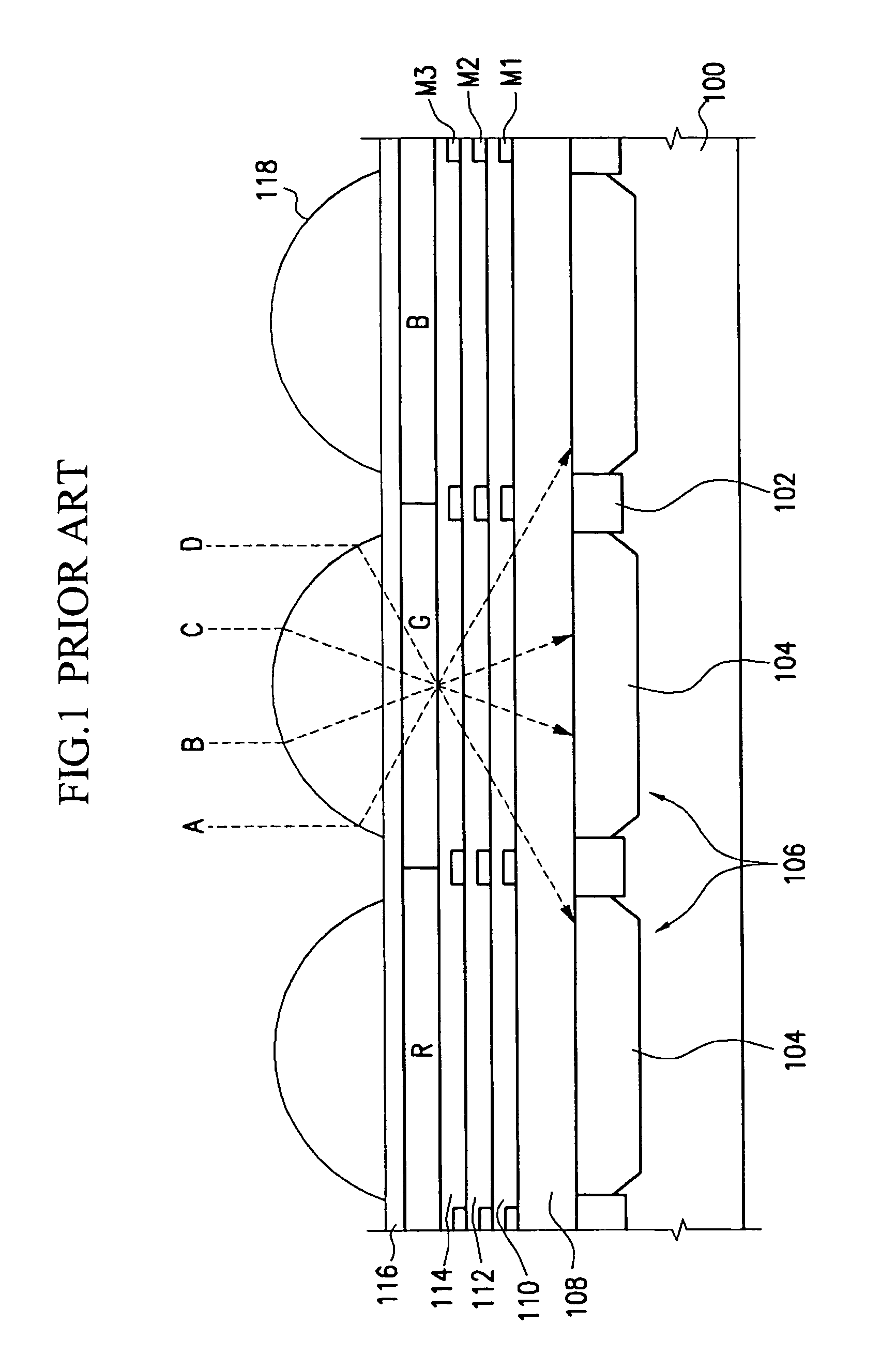
Such a phenomenon that light passing through the micro lenses 118 is incident on the CMOS devices of adjacent pixels, referred to as “cross talk,” produces unnecessary noise components, thereby deteriorating characteristics of the CMOS image sensor.
However, the image sensors disclosed in these patents have restrictions on effective avoidance of the cross talk.

Method used


Image

  • Complementary metal oxide semiconductor image sensor having cross talk prevention and method for fabricating the same
  • Complementary metal oxide semiconductor image sensor having cross talk prevention and method for fabricating the same
  • Complementary metal oxide semiconductor image sensor having cross talk prevention and method for fabricating the same

Examples


Embodiment Construction

[0024]Reference will now be made in detail to exemplary embodiments of the invention, examples of which are illustrated in the accompanying drawings. Wherever possible, the same reference numbers will be used throughout the drawings to refer to the same or like parts.

[0025]An embodiment of the present invention will now be described in detail with reference to the accompanying drawings.

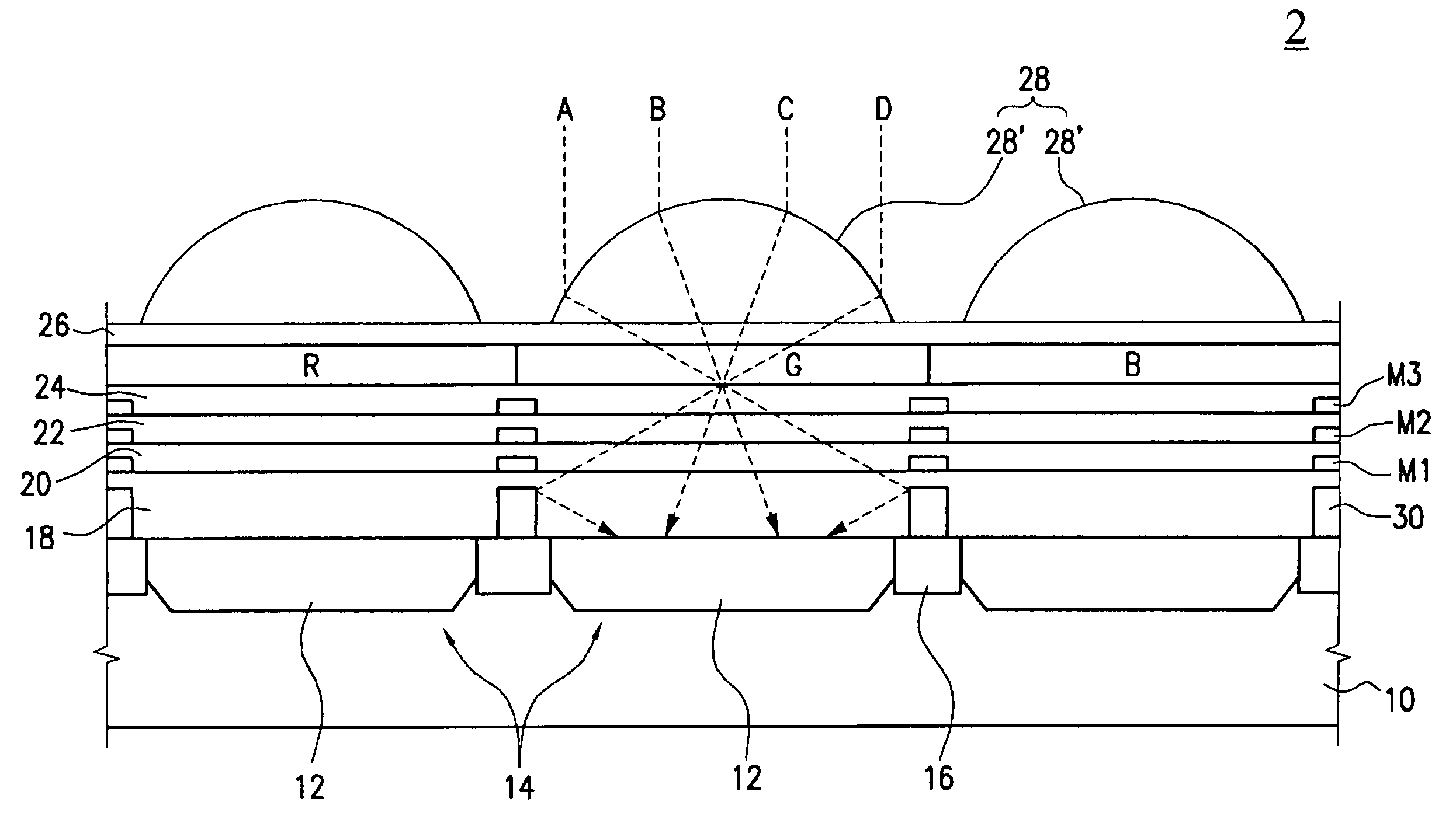
[0026]FIG. 2 is a schematic sectional view illustrating a CMOS image sensor 2 consistent with an embodiment of the present invention.

[0027]Referring to FIG. 2, CMOS image sensor 2 includes a semiconductor substrate 10 on which CMOS devices 14 are formed. CMOS devices 14 include photocharge generating portions 12 for receiving light externally and for generating and accumulating charges. In one aspect, photocharge generating portions 12 comprise photodiodes each formed as an impurity junction layer, with one photodiode provided per pixel.

[0028]In addition, CMOS devices 14 are formed in a plurality of d...


PUM


Abstract

Disclosed are a complementary metal oxide semiconductor (CMOS) image sensor and a method for fabricating the same, which are capable of effectively preventing a cross talk effect. The CMOS image sensor includes a semiconductor substrate; device isolation regions provided on the semiconductor for defining device regions therebetween; photocharge generating portions provided on the device regions for receiving external light and for generating and storing electric charges; light concentrating portions provided over the photocharge generating portions for concentrating the external light onto corresponding photocharge generating portions; and cross talk preventing portions for preventing the light passing through the light concentrating portions from being incident onto adjacent photocharge generating portions.

Description

RELATED APPLICATION[0001]This application is related to and claims benefits of priority under 35 U.S.C. §119 to Korean Patent Application No. 10-2003-0068503, filed on Oct. 1, 2003, entitled “CMOS IMAGE SENSOR AND FABRICATION METHOD THEREOF,” the entire contents of which are expressly incorporated herein by reference.BACKGROUND[0002](a) Technical Field[0003]The present invention relates to a complementary metal oxide semiconductor (CMOS) image sensor and a method for fabricating the same, and, more particularly, to a complementary metal oxide semiconductor (CMOS) image sensor capable of effectively preventing a cross talk effect and a method for fabricating the same.[0004](b) Description of the Related Art[0005]In general, semiconductor image sensors are semiconductor devices for converting an optical image into electrical signals and may be a charge coupled device (CCD) image sensor or a CMOS image sensor. Research efforts have been made to increase photosensitivity of the image se...

Claims


Application Information

Patent Timeline
Patent Type & Authority Patents(United States)
IPC IPC(8): H01L27/00H01J3/14H01L27/146H01L31/00
CPCH01L27/14603H01L27/14625H01L27/14621H01L27/1463H01L27/14627H01L27/146
Inventor JEON, IN-GYUN
Owner DONGBU ELECTRONICS CO LTD
Learn More